When the combined logic that produces the gated clock exceeds one level (ie, exceeds a single AND gate or OR gate), the reliability of the design project becomes difficult. Even if the prototype or simulation results do not show a static danger, there may still be dangers. In general, we should not use multi-level combinatorial logic to clock the flip-flops in a PLD design.
Figure 7 shows an example of a multi-level clock with a dangerous image. The clock is output by a multiplexer controlled by the SEL pin. The input to the multiplexer is the clock (CLK) and the divide by 2 (DIV2) of the clock. As seen from the timing waveform diagram of Fig. 7, in the case where both clocks are logic 1, when the state of the SEL line changes, there is a static danger. The extent of the danger depends on the conditions of the job. The danger of multi-level logic can be removed. For example, you can insert "redundant logic" into your design project. However, the PLD/FPGA compiler removes these redundant logic during logic synthesis, making it difficult to verify that the danger is actually removed. To this end, other methods must be sought to achieve the function of the circuit.
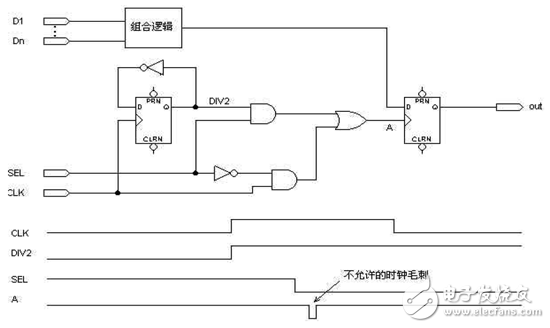
Figure 7 Multi-level clock with static danger
Figure 8 shows an alternative to a single stage clock of the Figure 7 circuit. The SEL pin and DIV2 signal in the figure are used to enable the enable input of the D flip-flop instead of the clock pin for the flip-flop. The use of this circuit does not require the logic unit of the additional PLD, but the work is much more reliable. Different systems require different methods to remove multi-level clocks, and there is no fixed mode.
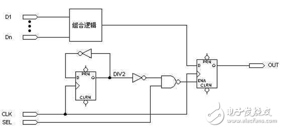
Figure 8. Multi-level clock with no static image (this circuit is logically equivalent to Figure 7, but more reliable)
2.6.4 Traveling Wave ClockAnother popular clock circuit uses a traveling wave clock, where the output of one flip-flop is used as the clock input for the other flip-flop. If carefully designed, the traveling wave clock can work as reliably as a global clock. However, the traveling wave clock complicates the circuit-related timing calculations. The traveling wave clock generates a large time offset between the clocks of the flip-flops on the traveling wave chain, and will exceed the worst-case setup time, hold time, and clock-to-output delay in the circuit, making the actual system The speed is decreasing.
When using an inverted flip-type flip-flop to form an asynchronous counter, a traveling wave clock is often used. The output of one flip-flop clocks the input of the next flip-flop. Referring to Figure 9, the synchronous counter is usually a better alternative to the asynchronous counter, because both require There are also many macrocells and the sync counter has a faster clock to output time. Figure 10 shows a synchronous counter with a global clock, which has the same function as Figure 9, with the same number of logic units, but with a faster clock-to-output time. Almost all PLD development software offers a wide variety of sync counters.
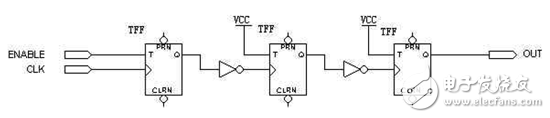
Figure 9 Traveling Wave Clock
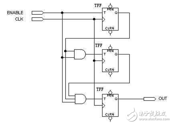
Figure 10 The traveling wave clock is converted into a global clock
(This 3-bit counter is an alternative to the asynchronous counter in Figure 9. It uses the same 3 macrocells but has a shorter clock-to-output delay)
2.6.5 Multi-clock systemMany systems require multiple clocks within the same PLD. The most common example is the interface between two asynchronous microprocessors, or the interface between a microprocessor and an asynchronous communication channel. Since a certain setup and hold time is required between the two clock signals, the above application introduces additional timing constraints. They also require synchronization of some asynchronous signals.
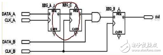
Figure 11 shows an example of a multi-clock system. CLK_A is used to clock REG_A, CLK_B is used to clock REG_B. Since REG_A drives the combination logic into REG_B, the rising edge of CLK_A has a settling time and hold time requirement relative to the rising edge of CLK_B. Since REG_B does not drive the logic fed to REG_A, the rising edge of CLK_B has no settling time requirement relative to CLK_A. In addition, since the falling edge of the clock does not affect the state of the flip-flop, there is no time requirement between the falling edges of CLK_A and CLK_B. As shown in Figure 4, 2. As shown in II, there are two independent clocks in the circuit, but the setup time and hold time requirements between them are not guaranteed. In this case, the circuit must be synchronized. Figure 12 shows how the value of REG_A (how to use it) is synchronized with CLK_B. The new trigger REG_C is touched by GLK_B, ensuring that the output of REG_G conforms to the setup time of REG_B. However, this method delays the output by one clock cycle.
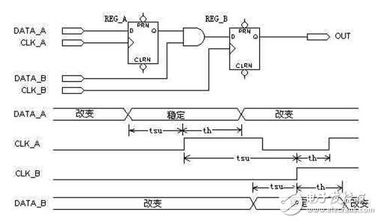
Figure ll Multi-clock system (timing waveform shows that the rising edge of CLK_A has a settling time and hold time constraint with respect to the rising edge of CLK_B)
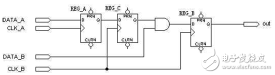
Figure 12 Multi-clock system with synchronous register output (if CLK_A and CLK_B are independent of each other, the output of REG-A must be synchronized with REG_C before it is fed to 1REG_B)
Synchronization of asynchronous signals is not enough in many applications. When there are two or more non-homologous clocks in the system, the setup and hold time of the data is difficult to guarantee, and we will face complicated time problems. The best way is to synchronize all non-homologous clocks. Using a lock ring (PLL or DLL) inside the PLD is a good method, but not all PLDs have PLLs, DLLs, and chips with PLL functions are mostly expensive, so unless there are special requirements, general occasions PLDs with PLLs may not be used. At this point we need to use a D flip-flop with an enable and introduce a high frequency clock.
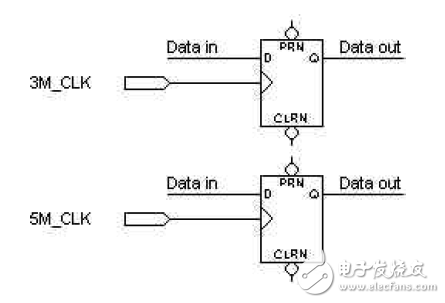
Figure 13 different source clocks
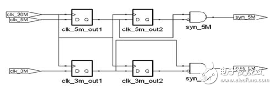
As shown in Figure 13, the system has two different source clocks, one for 3MHz and one for 5MHz. Different triggers use different clocks. For system stability, we introduced a 20MHz clock to synchronize the 3M and 5M clocks, as shown in Figure 15. The 20M high frequency clock will be used as the system clock and input to the clock terminals of all flip-flops. 3M_EN and 5M_EN will control the enable of all flip-flops. That is, the trigger connected to the 3M clock is connected to the 20M clock, and 3M_EN will control the trigger to be enabled. The trigger connected to the original 5M clock is also connected to the 20M clock, and 5M_EN will control the trigger to be enabled. This way we can synchronize any non-homologous clocks.
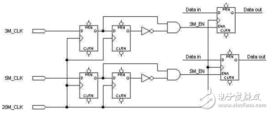
Figure 14 Synchronize any non-homologous clock
(A DFF and a back non-gate, the AND gate constitutes a clock rising edge detection circuit)
In addition, the asynchronous signal input can not always meet the data setup and hold time, and it is easy to make the system enter the metastable state. Therefore, it is also recommended that the designer synchronize all asynchronous inputs through the double trigger.
Summary: A stable and reliable clock is an important condition for the system to be stable and reliable. We cannot use any output that may contain glitch as a clock signal, and use only one global clock as much as possible. For multi-clock systems, pay attention to synchronous asynchronous signals and non-homologous. clock.
2.6.6 Some methods of multi-clock system design:If there is a fixed frequency multiple between the clocks, in this case their phases generally have a fixed relationship and can be processed as follows;
Use a high frequency clock as the operating clock and a low frequency clock as the enable signal. This is recommended when power consumption is not the primary factor;
Describe the circuit at the two clock transitions on the basis of careful analysis of the timing;
If there are two clocks of different frequencies in the circuit and the frequency is independent, the following strategy can be used:
The high frequency clock is used to sample two clocks, and the high frequency clock is used as the working clock of the circuit in the circuit, and the sampled low frequency clock is used as an enabler;
Two synchronization methods in the clock synchronization unit
Use handshake signal
Data buffering with dual clock FIFO
Clock synchronization, if there are two clocks clk_a and clk_b in the system, the designer can use the clock with frequency higher than max(clk_a, clk_b) twice as the sampling clock. The two low frequency clocks can be processed as triggers. The advantage of using this scheme is that the whole circuit works with a single clock, but requires an extra high-frequency clock. When the circuit has power requirements, the designer should carefully consider it;
Using 20M sampling 3M and 5M, syn_5M as the enable signal of the original 5M signal driving register;
Sampling 2 low frequency clock schematics using high frequency clock
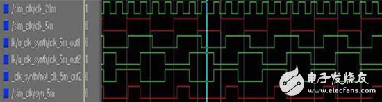
Sampling 2 low frequency clock waveforms using high frequency clock
When synchronizing modules between modules that are controlled by two different system clocks, the following principles should be observed: There should be no more logic between the two registers operating with different clocks, but only a connection. As shown in the figure below, this method is beneficial to control the satisfaction of establishing the hold time.
The handshake signal mechanism is the basic way of communication between asynchronous systems. We can also use this method when dealing with interfaces between different clocks, but it should be noted that the designer should carefully analyze the effective duration of the handshake and response signals. Make sure the sampled data is correct.
At present, the dual clock FIFO macro unit provided in various devices provides good access to the asynchronous dual clock. The unit has two circuits for coordinating two clocks to ensure correct reading and writing. This device can be used to synchronize data.
1. Use a global clock and do not involve the clock in the operation. The system provides a certain number of global clock lines. When laying out the wiring, try to meet the requirements of these signals to reduce the clock offset and tilt. If the timing is unreasonable and more gated clocks are used, the skew of these clocks will be larger, and the setup time and hold time cannot be guaranteed, resulting in a decrease in the operating frequency of the circuit or inability to work.
2. Divide the working module by register. When designing a large-scale circuit, the sub-module design is indispensable, and the system is coordinated after each module is passed. However, due to the different tension of the wiring resources during single-module debugging and joint debugging, the output of each module cannot be kept the same as that of the individual wiring, which causes difficulties in joint debugging. If the output port of each module adopts the register output, the output of each module can guarantee the original timing even after the overall layout and wiring, which greatly improves the working efficiency of the joint debugging. Adding these registers also increases the testability of the circuit.
3. The combinatorial logic tries to adopt the parallel structure as much as possible. Reducing the delay of the combined path between registers is the most important means to improve the operating frequency of the system. Therefore, parallel logic should be used as much as possible under the premise of completing the same function, as shown in Figure 6.
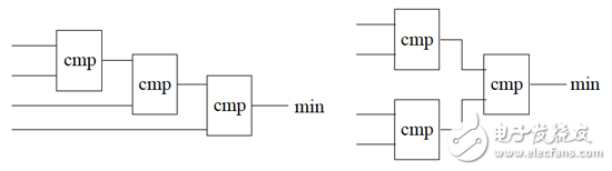
Figure 6 Serial and parallel implementation of a four-input comparator
If there is no priority requirement, it should be described by case statement, so that the integrated circuit parallelism is larger. If the if-then-else structure is adopted, the integrated circuits are serial, which increases the delay path.
4. The latch should be eliminated in the description. If a certain data needs to be saved, the register should be arranged reasonably, because the latch is sensitive to the input during the entire working level, and any glitch in the input passes through the latch. It will not be eliminated, which will greatly increase the possibility of competitive competition in the subsequent combined circuits, affecting circuit performance. Some inappropriate descriptions also cause unnecessary latches to be added, increasing the area of ​​the circuit.
5. Synchronous design should be used in the design. The signal is sampled by the clock and then participate in the logic operation. This can block the combined path and eliminate the glitch. In the design, the output of the combined signal does not allow feedback as an input to the combinatorial logic, thus avoiding the combined loop.
tcl , https://www.tclgroupss.com