Note: Synthesizers tend to optimize when using multi-level NOT gates, because the synthesizer will consider a signal not twice or itself.
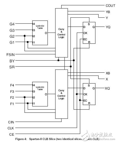
It should be noted that the internal structure of the FPGA/CPLD is a standard macrocell. The figure below is a standard macrocell of the Xilinx Spartans II family of devices. Although the chip macrocells of different manufacturers have different structures, they are generally composed of some combinatorial logic plus one or two flip-flops. In practical applications, when the combinatorial logic in a module is used, the corresponding flip-flop cannot be used; if the trigger unit is used, the combinatorial logic unit is also invalid. This is sometimes the case (especially with CPLDs). Although the design uses few resources, the place router reports the lack of resources.
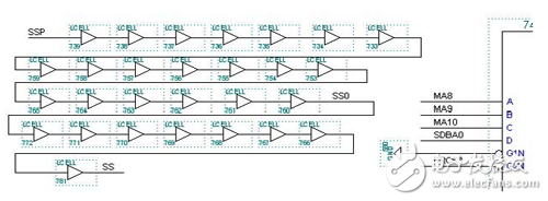
An example of this is a design that I encountered in the company some time ago. Designed using Altera's EPM7256 model CPLD. The design actually uses only 109 register resources, accounting for 42% of the total device resources. However, the design uses the delay method shown below to make the timing of the processor interface:
An example of this is a design that I encountered in the company some time ago. Designed using Altera's EPM7256 model CPLD. The design actually uses only 109 register resources, accounting for 42% of the total device resources. However, the design uses the delay method shown below to make the timing of the processor interface:
A large number of LCELLs are used in the design of this circuit to generate a delay of more than 100 nanoseconds. The consequence of this is that although the entire circuit's trigger resources are only 42% used, the layout and routing with MaxplusII can not pass. . And I suspect that the signal generated after so many logical delays can still maintain the original performance.
When it is necessary to delay a certain signal, beginners often connect some non-gates or other gate circuits after this signal. This method is feasible in the separation circuit. However, in the FPGA, the development software will remove these gates as redundant logic in the integrated design, and the delay effect will not be achieved. When developing an FPGA with ALTERA's Maxplus II, a certain delay can be generated by inserting some LCELL primitives, but the delay thus formed is unstable in the FPGA chip and changes with the external environment such as temperature, so This is not recommended. Here, a high-frequency clock can be used to drive a shift register, and the delay signal is used for data input. The number of stages of the shift register is correctly set according to the required delay, and the output of the shift register is the delayed signal. The delay signal generated by this method has an error from the original signal, and the error is determined by the period of the high frequency clock. For the delay of the data signal, the error can be eliminated by resampling the delayed signal with the data clock at the output.
The recommended method for such a large delay is to use a clock latch to generate the delay. We know that when a signal is latched once with a clock, it will occupy a trigger resource and the signal will go backward one clock cycle. In the design of the colleague, the CPLD chip is connected with a 32MHz clock, so the ssp signal is shifted by 31ns every time the clock is latched, so that only three more trigger resources can be used to achieve the goal. The circuit diagram and simulation waveform are shown in the following figure: Of course, this will slightly change the width of the original signal high and low levels, but it will not affect the implementation of the function as long as it is within the tolerance of the chip with which it is interfaced.
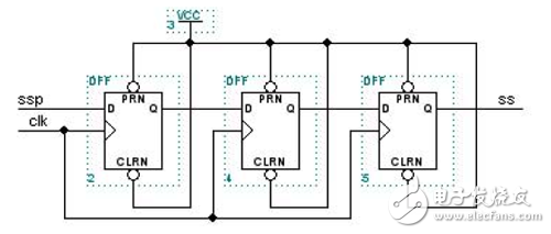
Circuit diagram for delay
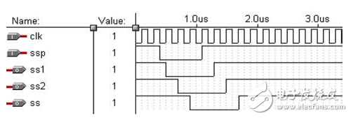
The above simulation waveform
2.3 How to improve the running speed of the system
The speed of the synchronization circuit refers to the speed of the synchronous clock. The faster the synchronous clock, the shorter the time interval between the processing of data by the circuit, and the larger the amount of data processed by the circuit per unit time.
Let's take a look at a basic model of data transfer in a synchronous circuit, as shown below:
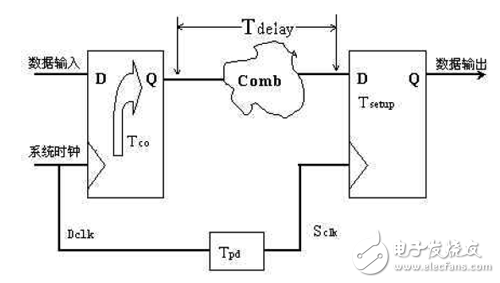
(Tco is the delay from the trigger clock to the data output; Tdelay is the delay of the combinatorial logic; Tsetup is the trigger setup time)
Assuming that the data has been driven into the D flip-flop by the rising edge of the clock, then the data reaches the Q end of the first flip-flop and the T-end of the second flip-flop that arrives at the delay of the combined logic Tdelay. The second trigger can be locked into the trigger again, the clock delay can be no later than Tco+Tdelay+Tsetup, (we can review the concept of setup and hold time mentioned earlier, you can understand why the formula Finally add a Tdelay) From the above analysis, the minimum clock cycle: T = Tco + Tdelay + Tsetup The fastest clock frequency F = 1 / T PLD development software is also used to calculate the system operating speed Fmax.
Note: There is a parameter in this logic diagram: Tpd, which is the delay parameter of the clock. We did not mention this parameter when we just did time analysis. (If you use the global clock model of PLD, Tpd can be 0, if it is Ordinary clock is not 0). So if you consider the delay of the clock, the exact formula should be T = Tco + Tdelay + Tsetup - Tpd. Of course, all of the above analysis is the internal operating speed of the device. If you consider the impact of the chip I/O pin delay on the system speed, you need to add some corrections.
Lead Acid vs. Lithium: Safety
Safety is always a primary consideration when designing a solar system, but it becomes even more important when your system is on a boat far from shore, or an RV on a remote road. Different battery chemistries have different risk factors. Obviously, abusing any type of battery can create a dangerous situation. But with normal, and perhaps even a bit of rough treatment, the different batteries have different safety concerns that need to be addressed.
- Flooded lead acid batteries have an acid and water electrolyte in the battery that has to be checked on a regular basis. During normal charging cycles, this mixture turns into a gas that needs to be vented outside. A buildup of the gas inside a vehicle or vessel can be explosive. Proper ventilation mitigates this concern. The outgassing of the battery is normal, but requires owners to regularly check to see when the electrolyte level gets low from the outgassing. If low, it needs to have more distilled water added. This runs the risk of acid spills if overfilled or overcharged. This requires you to be prepared with proper safety equipment including gloves, safety glasses, and baking soda to neutralize the acid if needed.
- Sealed lead acid batteries do not have outgassing or electrolyte levels to check, as they do not outgas. Normal battery safety measures should be followed, like checking for tight cable connections, corrosion, and preventing physical damage to the battery itself.
- Lithium batteries also do not outgas, but certain types (the ones with cobalt, known as lithium cobalt oxide or LCO) can experience thermal runaway – a condition where the battery starts to get hot, which causes it to react to the heat and get hotter and hotter until it catches on fire. LCO batteries are most commonly used in cell phones, hoverboards, and electric cars, and are generally not recommended for mobile applications.
Storage Battery Pack,Power Pack Home,Battery Storage Pack,Battery Pack Storage
Shenzhen Sunbeam New Energy Co., Ltd , https://www.sunbeambattery.com