In recent years, there has been a growing interest in radio frequency (RF) CMOS processes and the associated RF models that support them. This article aims to delve into the significance of these RF technologies and why they are essential for modern RF circuit design. As the demand for high-frequency applications increases, understanding the differences between traditional digital CMOS and RF CMOS becomes more critical than ever.
When approaching RF CMOS design, we can break it down into three main perspectives. First, low-frequency analog designers are increasingly moving their designs to higher frequencies, requiring a deeper understanding of RF behavior. Second, discrete RF/microwave engineers are shifting toward integration, leveraging CMOS technology for more compact and efficient systems. Third, digital designers are pushing serial data interfaces like SERDES to the highest frequencies supported by the process. In all these cases, RF CMOS plays a vital role, and we will explore how its modeling differs from conventional approaches.
Substrate
Traditional CMOS for digital applications typically uses low-resistivity bulk substrates with a thin, high-resistivity epitaxial layer. This configuration is optimized for latch-up performance and manufacturing yield. However, when it comes to RF design, this setup presents several challenges.
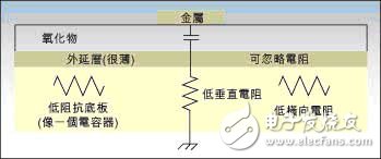
Figure 1: Basic digital CMOS model built on a low resistivity bulk substrate
For digital circuits, multiple metal layers are often designed with uniform thickness to allow consistent routing across all layers. This works well for digital applications but poses problems for RF designers. The low-resistivity substrate leads to significant parasitic capacitance, which can degrade RF performance. Additionally, the coupling between inductors and the grounded substrate reduces inductance and Q-factor, while current flow through the substrate can cause unwanted interference.
To address these issues, RF CMOS processes often use a high-resistivity epitaxial layer throughout the substrate. This creates a second, smaller capacitor in series with the parasitic capacitance, effectively increasing the overall impedance. As a result, parasitic effects are reduced, and the Q-factor of inductors improves significantly. Moreover, using thicker or higher-conductivity metal layers—such as copper—can further enhance performance.
BSIM3 Model
The BSIM3 model is one of the most widely used device models in CMOS design. It combines physical and empirical parameters, making it adaptable to new fabrication processes. While it's commonly used for digital circuits, RF designers must understand how it behaves at higher frequencies.
Model parameter extraction typically involves fabricating test devices with different dimensions and measuring their DC and low-frequency characteristics. Capacitance measurements then fill in the capacitive parameters. These parameters are refined using tools like Hspice OpTImizer to ensure the model closely matches real-world performance. If discrepancies arise across different device sizes, the model may be split into multiple parameter sets, allowing better accuracy over a wider range of scales.
The compact nature of the BSIM3 model makes it suitable for fast simulations and layout tools, giving designers flexibility and precision. Understanding how this model behaves at RF frequencies is crucial for optimizing high-speed and high-frequency circuits.
Fiber Optic Distribution Box,Fiber Optic Breakout Box,Fibre Optic Breakout Box,Fibre Break Out Box
Cixi Dani Plastic Products Co.,Ltd , https://www.danifiberoptic.com