The simplified circuit diagram for the TPV S569P color display line output is shown below (the dashed lines indicate that some components are not fully depicted). The excitation circuit of this device employs a reverse polarity excitation method. Specifically, when the row excitation transistor V402 is activated, the output transistor V403 is deactivated, and vice versa. Given that the device supports multiple frequency scans, a FET with excellent shut-off characteristics was used for V402 to prevent increased power consumption at varying frequencies.
The row excitation transformer T401 provides V403 with a switching pulse current, enabling it to operate in a switching mode. If the current becomes too high, it could potentially damage the V403 transistor. To address this, a current-limiting resistor R428 and a shunt resistor R427 were added in series on the b terminal of V403. Additionally, R427 forms a bleeder circuit with VD405.
During the turn-on phase of V402, the positive and negative pulse voltages induced on the secondary winding of T401 are discharged via R427 and VD405, preventing excessive reverse currents from damaging the V403 transistor. C415 and R425 form a damping circuit to protect against excessive D-peak voltage during the V402 cutoff period.
When V403 is conducting in saturation, the B+ voltage replenishes the magnetic energy in the primary winding (windings 1-2) of the output transformer T402. The stored energy in the S-correction capacitor C425 passes through the T402 primary winding and the row deflection coil H. This energy is then grounded through the output of the line output transistor V403 and the DY component. At this point, the magnetic field generated in H.DY guides the electron beam to complete the scanning from the center of the raster to the right side. During the V403 cutoff period, the current in H.DY cannot change abruptly, inducing an electromotive force in H.DY. The line-reverse capacitors C418 and C419 charge up, reaching their maximum voltage as the charging current decreases to zero. The voltage across C418 and C419 gradually discharges back to zero via H.DY, completing the reverse retrace process until the current in H.DY reaches its reverse peak, converting all electrical energy into magnetic energy.
At this stage, the dual-damper tube VD408, composed of two Schottky diodes, becomes positively biased. The current in H.DY forms a loop through VD408, guiding the electron beam to complete the scanning from the center of the raster to the left side.
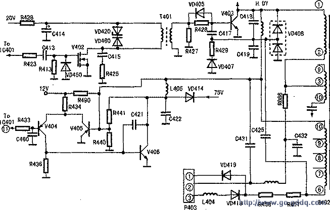
Overall, this circuit design ensures efficient operation and protection of key components like V403 and T402, allowing for smooth scanning across the display. The integration of various resistors, capacitors, and diodes creates a robust system capable of handling different operational conditions without compromising performance. Furthermore, the use of advanced components such as the industrial router crystal and MOS power ICs highlights the sophistication of the design, ensuring reliability and precision in the color display system. The damping circuits and protective measures further demonstrate the attention to detail in engineering this device, making it a reliable choice for demanding applications.
Core Drill Sand Blasting Machine,Automatic Diamond Sandblasting Machine,Saw Blade Sand Blasting Machine,Diamond Saw Blade Sand Blasting Machine
Suzhou Mountain Industrial Control Equipment Co., Ltd , https://www.szmountain.com