With the development of semiconductor technology, computer technology and communication technology, the field of industrial control has undergone earth-shaking changes, and it is constantly developing and is moving towards new technologies. At present, logic devices can be divided into two categories: fixed logic devices and programmable logic devices: circuits in fixed logic devices are permanent, they perform one or a group of functions, and once they are manufactured, they cannot be changed; Programmable Logic Devices (PLDs) are standard finished components that offer customers a wide range of logic capacity, characteristics, speed and voltage parameters, and can be changed at any time to perform many different functions.
For fixed logic devices, the time required from design, prototype to final production can vary from a few months to more than a year, depending on the complexity of the device. If the device is not working properly, or if the application requirements change, then a completely new design must be developed. The preliminary work of designing and verifying fixed logic requires a large amount of NRE cost.
For programmable logic devices, designers can quickly develop, simulate, and test their designs with inexpensive software tools. The design can then be quickly programmed into the device and the design tested immediately in the actual running circuit. The PLD device used in the prototype is identical to the PLD used to form the final device. This eliminates the cost of NRE and the final design is faster than with custom fixed logic.
Five advantages of PLD
Fixed logic devices and PLDs each have their own advantages. For example, fixed logic devices are often more suitable for high volume applications because they can be mass produced more economically. For some applications that require extreme performance, fixed logic may also be the best choice. However, programmable logic devices offer some important advantages over fixed logic devices, including:
First, it provides customers with greater flexibility in the design process, because for PLD, design iterations only need to simply change the programming file, and the results of the design changes can be seen immediately in the working device.
Second, there is no need for a long lead time to make prototypes or official products. PLD devices are already on the distributor's shelves and can be shipped at any time.
Third, there is no need for customers to pay high NRE costs and purchase expensive mask sets. PLD vendors have already paid for these costs when designing their programmable devices, and they can share these costs through the lifetime of the PLD product line.
Fourth, allowing customers to order only the quantity they need when needed, so that customers can control inventory. Customers using fixed logic devices often face excess inventory that needs to be discarded, and when demand for their products is high, they may suffer from a shortage of devices and have to face the reality of production delays.
Fifth, the PLD can be reprogrammed even after the device is shipped to the customer. In fact, with programmable logic devices, some device manufacturers are now trying to add new features or upgrades to products already on site. To achieve this, new hardware logic can be created in the system by simply uploading new programming files to the PLD over the Internet.
Equally important, PLDs are now supported by an increasing number of core technology (IP) libraries that allow users to quickly implement system functions within PLDs using these predefined and pre-tested software modules. The IP core includes everything from complex digital signal processing algorithms and memory controllers to bus interfaces and sophisticated software microprocessors. This type of IP core saves customers a lot of time and money.
CPLD and FPGA comparison
Two types of programmable logic devices are Field Programmable Gate Arrays (FPGAs) and Complex Programmable Logic Devices (CPLDs). Among these two types of programmable logic devices, FPGAs are further developed on the basis of programmable devices such as PAL, GAL, and EPLD. It emerged as a semi-custom circuit in the field of application specific integrated circuits (ASIC), which not only solves the shortcomings of the custom circuit, but also overcomes the shortcomings of the limited number of original programmable device gates.
FPGA adopts a new concept of logic cell array LCA, which includes three parts: configurable logic module CLB, output input module IOB and internal connection. The basic features of FPGA are:
1) FPGA design ASIC circuit, users do not need to cast film production, you can get a shared chip.
2) The FPGA can be used as a mid-sample for other fully custom or semi-custom ASIC circuits.
3) There are a lot of flip-flops and I/O pins inside the FPGA.
4) FPGA is one of the devices with the shortest design cycle, lowest development cost and lowest risk in ASIC circuits.
5) FPGA adopts high-speed CHMOS technology, low power consumption, and can be compatible with CMOS and TTL levels.
It can be said that the FPGA chip is one of the best choices for improving the system integration and reliability of small batch systems. At present, there are many varieties of FPGAs, such as the XC series of XILINX, the FIEX series of ALTERA, and the CME-M series of Jingweiyag.
The FPGA is set up by the program stored in the on-chip RAM, so the on-chip RAM needs to be programmed during operation. Different programming modes can be used according to different configuration modes. When power is applied, the FPGA chip reads the data in the EPROM into the on-chip programming RAM. After the configuration is completed, the FPGA enters the working state. After the power is turned off, the FPGA is restored to a white chip, and the internal logic relationship disappears. Therefore, the FPGA can be used repeatedly. The FPGA programming does not require a dedicated FPGA programmer, just a general EPROM, PROM programmer. When you need to modify the FPGA function, you only need to change one EPROM. In this way, the same FPGA, different programming data, can produce different circuit functions. Therefore, the use of FPGAs is very flexible.
FPGA has multiple configuration modes: parallel main mode is a piece of FPGA plus one EPROM mode; master-slave mode can support one piece of PROM to program multiple FPGAs; serial mode can use serial PROM to program FPGA; peripheral mode can use FPGA as micro A peripheral to the processor that is programmed by the microprocessor.
At the same time, CPLD provides much less logical resources, up to about 10,000 gates. However, CPLDs provide very good predictability and are therefore ideal for critical control applications. Moreover, CPLD devices require extremely low power and are inexpensive, making them ideal for cost-sensitive, battery-powered portable applications.
to sum up:
The value of programmable logic is that it shortens the electronics manufacturer's development cycle and the ability to get their products to market faster. High-performance FPGAs are now gaining market share from fixed logic devices built with state-of-the-art standard cell technology. According to data from the Semiconductor Industry Alliance (SIA), programmable logic is now one of the fastest growing segments of the semiconductor industry, with PLD sales growing faster than the average sales growth of the entire semiconductor industry.
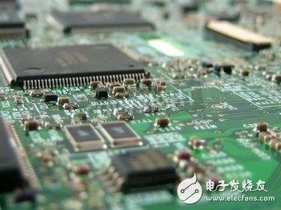
HDI PCB Specification
High density interconnect (HDI) PCBs represent one of the fastest-growing segments of the printed circuit board market. Because of its higher circuitry density, the HDI PCB design is able to incorporate finer lines and spaces, smaller vias and capture pads, and higher connection pad densities. A high density PCB features blind and buried vias and often contains microvias that are .006 in diameter or even less.
HDI PCBs are characterized by high-density attributes including laser microvias, fine lines and high performance thin materials. This increased density enables more functions per unit area. Higher technology HDI PCBs have multiple layers of copper filled stacked microvias (Advanced HDI PCBs) which creates a structure that enables even more complex interconnections. These very complex structures provide the necessary routing solutions for today's large pin-count chips utilized in mobile devices and other high technology products.
The HDI PCBs we offer include the following highly requested characteristics:
Blind and/or buried vias
Via-in-pad
Through vias from surface to surface
20 µm circuit geometries
30 µm dielectric layers
50 µm laser vias
125 µm bump pitch processing
Applications
HDI PCB is used to reduce size and weight, as well as to enhance electrical performance of the device. HDI PCB is the best alternative to high layer-count and expensive standard laminate or sequentially laminated boards. HDI incorporate blind and buried vias that help to save PCB real estate by allowing features and lines to be designed above or below them without making a connection. Many of today's fine pitch BGA and flip-chip component footprints do not allow for running traces between the BGA pads. Blind and buried vias will only connect layers requiring connections in that area.
HDI PCB
HDI PCB,Special HDI PCB,HDI Prototype PCB,HDI Board PCB
Storm Circuit Technology Ltd , https://www.stormpcb.com