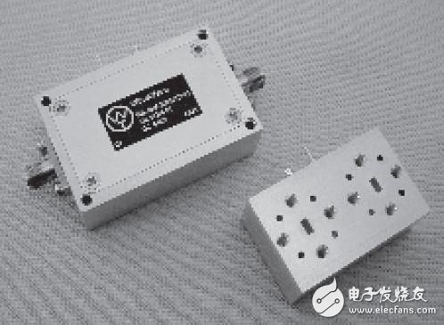
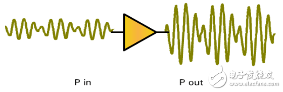
RF power amplifiers (RF PAs) play a crucial role in wireless communication systems, serving as key components in the transmitter chain. The RF signal generated by the modulating oscillator is typically weak and must go through several stages of amplification—starting with the pre-amplifier, then the intermediate amplifier, and finally the power amplifier stage—to achieve sufficient output power before being transmitted via an antenna. Without an RF power amplifier, it would be impossible to generate the necessary high-power RF signals required for effective transmission.
 RF amplifiers can be categorized into different types based on their function and performance. These include high-gain amplifiers, low-noise amplifiers, and medium-to-high power amplifiers. At the core of these circuits lies a microwave transistor, which enables efficient amplification at high frequencies.
RF power amplifiers operate at high frequencies, but their bandwidth is relatively narrow. To maintain signal integrity, they often use frequency-selective networks as part of their load circuit. Depending on the conduction angle of the current, RF power amplifiers are classified into three main operating modes: Class A, Class B, and Class C. In Class A amplifiers, the current flows for the entire cycle (360°), making them ideal for small-signal applications. Class B amplifiers have a conduction angle of 180°, while Class C amplifiers have a conduction angle less than 180°. Class B and C are more suitable for high-power operations. Among these, Class C amplifiers offer the highest efficiency and output power, though they produce significant waveform distortion. This distortion is mitigated by using a tuned circuit as the load, which filters out harmonics and ensures a cleaner output signal.
RF amplifiers can be categorized into different types based on their function and performance. These include high-gain amplifiers, low-noise amplifiers, and medium-to-high power amplifiers. At the core of these circuits lies a microwave transistor, which enables efficient amplification at high frequencies.
RF power amplifiers operate at high frequencies, but their bandwidth is relatively narrow. To maintain signal integrity, they often use frequency-selective networks as part of their load circuit. Depending on the conduction angle of the current, RF power amplifiers are classified into three main operating modes: Class A, Class B, and Class C. In Class A amplifiers, the current flows for the entire cycle (360°), making them ideal for small-signal applications. Class B amplifiers have a conduction angle of 180°, while Class C amplifiers have a conduction angle less than 180°. Class B and C are more suitable for high-power operations. Among these, Class C amplifiers offer the highest efficiency and output power, though they produce significant waveform distortion. This distortion is mitigated by using a tuned circuit as the load, which filters out harmonics and ensures a cleaner output signal.
 The structure of an RF amplifier generally includes three main sections: the input matching network, the output matching network, and the biasing circuit. Matching networks are essential for impedance matching between the amplifier and the source or load. Tools like ADS (Advanced Design System) can be used to design and simulate these networks, especially for narrowband applications. After initial simulation, fine-tuning is usually performed to optimize performance.
In many modern RF amplifier ICs, such as the AVAGO MGA30889 series, the matching circuit is already integrated within the chip. This simplifies the design process, requiring only the addition of DC-blocking capacitors. For example, capacitors C7 and C8 are used for DC blocking, while L1 and C8 form the DC biasing network. Additionally, C1, C2, and C3 serve as power supply filter capacitors to ensure stable operation.
DC-blocking capacitors are essential in RF amplifier circuits because they prevent DC voltage from reaching the RF signal path. Their value determines the cutoff frequency of the circuit. Smaller capacitors result in higher cutoff frequencies but may cause more high-frequency loss, while larger capacitors lower the cutoff frequency and reduce high-frequency loss. Similarly, the inductance in the biasing network affects the circuit's performance. Larger inductors lower the cutoff frequency but may introduce more harmonics, while smaller inductors improve high-frequency response. Typically, inductors above 100nH are used, and the inductor size should be chosen based on the supply current. For better gain flatness, tapered inductors combined with high-frequency capacitors can be used to enhance performance.
Overall, designing an RF power amplifier involves careful consideration of matching networks, biasing, and component selection to ensure optimal performance across the desired frequency range.
The structure of an RF amplifier generally includes three main sections: the input matching network, the output matching network, and the biasing circuit. Matching networks are essential for impedance matching between the amplifier and the source or load. Tools like ADS (Advanced Design System) can be used to design and simulate these networks, especially for narrowband applications. After initial simulation, fine-tuning is usually performed to optimize performance.
In many modern RF amplifier ICs, such as the AVAGO MGA30889 series, the matching circuit is already integrated within the chip. This simplifies the design process, requiring only the addition of DC-blocking capacitors. For example, capacitors C7 and C8 are used for DC blocking, while L1 and C8 form the DC biasing network. Additionally, C1, C2, and C3 serve as power supply filter capacitors to ensure stable operation.
DC-blocking capacitors are essential in RF amplifier circuits because they prevent DC voltage from reaching the RF signal path. Their value determines the cutoff frequency of the circuit. Smaller capacitors result in higher cutoff frequencies but may cause more high-frequency loss, while larger capacitors lower the cutoff frequency and reduce high-frequency loss. Similarly, the inductance in the biasing network affects the circuit's performance. Larger inductors lower the cutoff frequency but may introduce more harmonics, while smaller inductors improve high-frequency response. Typically, inductors above 100nH are used, and the inductor size should be chosen based on the supply current. For better gain flatness, tapered inductors combined with high-frequency capacitors can be used to enhance performance.
Overall, designing an RF power amplifier involves careful consideration of matching networks, biasing, and component selection to ensure optimal performance across the desired frequency range.
General Purpose Scanners,General Purpose Barcode Scanner,Ls2208 General Purpose Barcode Scanner,Symbol Ls2208 General Purpose Barcode Scanner
Guangzhou Winson Information Technology Co., Ltd. , https://www.barcodescanner-2d.com