TFT-LCD Introduction
What is TFT-LCD?
TFT: Thin-film transistor
LCD ﹕ Liquid crystal display
TFT-LCD was invented in 1960, and after continuous improvement, it was successfully commercialized as a notebook computer panel in 1991, and entered the TFT-LCD generation from then on.
TFT-LCD structure:
Simply put, the basic structure of a TFT-LCD panel is a layer of liquid crystal sandwiched between two glass substrates. A color filter is attached to the front LCD panel, and a thin film transistor (TFT) is fabricated on the rear TFT panel. When a voltage is applied to the transistor, the liquid crystal turns, and light passes through the liquid crystal to produce a pixel on the front panel. The backlight module is located behind the TFT-Array panel and is responsible for providing the light source. Color filters give each pixel a specific color. Combining each pixel of different colors presents the image on the front of the panel. 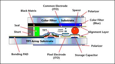
TFT Pixel Element:
A TFT panel is composed of millions of TFT devices and ITO ((In TI Oxide, this material is a transparent conductive metal) area arranged as a matrix, and the so-called Array is an area with millions of TFT devices arranged neatly The millions of neatly arranged areas are the panel display area. The following figure shows the structure of a TFT pixel 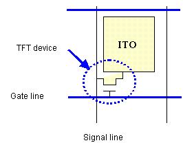
Regardless of the changes in the design of the TFT panel and the simplification of the manufacturing process, the structure must be equipped with a TFT device and a control liquid crystal area (if the light source is a transmissive LCD, the area for controlling the liquid crystal is ITO, but for the reflective LCD It is a metal with high reflectivity, such as Al, etc.)
TFT device is a switch, its function is to control the number of electrons to the ITO area. When the number of electrons flowing into the ITO area reaches the desired value, then turn off the TFT device, then turn off the entire electron ( Keep) in the ITO area. 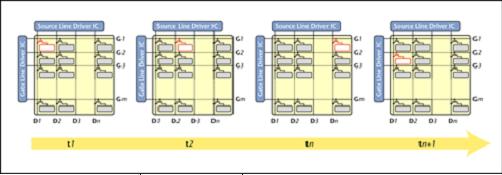
The picture above shows the specified time change of each pixel point. From t1 to tn, the gate driver IC continues to select G1 to enable the source driver IC to charge the TFT pixels on G1 in the order of D1, D2 to Dn. At tn + 1, the gate driver IC selects G2 again, and the source driver IC selects D1 in sequence. 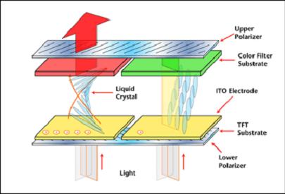
The above picture can express several things:
The more vertical the standing angle of the LCD, the more light will not be guided by the liquid crystal. The different standing angles of the LCD will guide different amounts of light. Taking the above example, the larger the standing angle of the LCD, the more it can penetrate The weaker the light. (The direction of the arrangement of the upper and lower polarizers will determine the strength of the transmitted light, so as long as you understand the strength of the light guided by the liquid crystal standing angle).
Unguided light will be absorbed by the upper polarizer. The polarity of light in nature is in any direction. The function of using a polarizer is to filter out most of the oscillating light in different directions and only let light in a certain direction pass.
New generation and size
What is the relationship between glass substrates and sizes of different generations?
Many people do not understand the differences between different generations of TFT-LCD industry plants. In fact, the principle is quite simple. The main difference between different generations of factories is the size of the glass substrate, and the panel is a product cut from a large glass substrate. The newer generation factories have larger glass substrates, so they can cut more panels to increase production capacity and reduce costs, or they can produce larger-sized panels (such as LCD TV panels).
In the 1990s, the TFT-LCD industry had just emerged in Japan. At that time, Japan designed and built a manufacturing plant (referred to as G1) process. The glass substrate of the first-generation factory is about 30 X 40 cm in size, which is equivalent to a full-open magazine and can be made into a 15-inch panel. When Daqi Technology (later merged with Lianyou Optoelectronics into AUO Optoelectronics) entered the industry in 1996, the technology had advanced to the 3.5th generation factory (G3.5), and the size of the glass substrate was about 60 X 72 cm. So far, AU Optronics has developed to the sixth-generation (G6) manufacturing process, and the size of the G6 glass substrate has reached 150 X 185 cm, which is equivalent to the size of a double bed. A G6 glass substrate can cut 30 15-inch panels. Compared to G3.5 which can cut 4 panels, G1 can only make 1 15-inch panel. The capacity of the sixth-generation factory is enlarged by multiples, and the relative cost reduce. In addition, the large size of the G6 glass substrate can also be cut into large-size panels, which can produce 8 32-inch LCD TV panels, which improves the diversity of panel product applications. Therefore, global TFT-LCD manufacturers have all invested in the process technology of the new generation plant.
TFT-LCD process introduction
What is TFT-LCD?
TFT-LCD is the abbreviation of thin-film transistor liquid-crystal display. (Thin-film transistor liquid crystal display) How does TFT-LCD light up? Simply put, a TFT-LCD panel can be regarded as a layer of liquid crystal sandwiched between two glass substrates The upper glass substrate is connected with a color filter (Color Filter), and the lower glass has transistors embedded on it. When the current through the transistor changes the electric field, causing the liquid crystal molecules to deflect, thereby changing the polarization of the light, and then using the polarizer to determine the light and dark state of the pixel (Pixel). In addition, because the upper glass is attached to the color filter, each pixel contains three colors of red, blue, and green. These pixels that emit red, blue, and green colors form the image on the panel.
The three main processes of TFT-LCD:
Front Array
-The previous Array process is similar to the semiconductor process, but the difference is that the thin film transistors are made on glass instead of silicon wafers.
Middle Cell
-The middle Cell is the glass of the previous Array as the substrate, combined with the glass substrate of the color filter, and the liquid crystal (LC) is poured between the two glass substrates.
Module Assembly (Modular Assembly)
-The back-end module assembly process is the production operation of assembling the glass after the Cell process with other components such as backlight boards, circuits, and outer frames.
-
Latest technology development
Organic light emitting display
Organic Light Emitting Display (Organic Light EmitTIng Display) or Organic Light Emitting Diode (Organic Light EmitTIng Diode), referred to as OLED for short, this technology has the following superior use characteristics.
l Self-illumination
l Ultra-thin features
l High brightness
l High luminous efficiency
l High contrast
l Microsecond response time
l Super wide viewing angle
l Low power consumption
l Wide temperature range
l Flexible panel
l Low temperature polysilicon
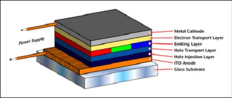
The principle of luminescence is to vapor-deposit an organic film between a transparent anode and a metal cathode, inject electrons and holes, and use it to recombine between the organic films to convert energy into visible light. And it can be matched with different organic materials to emit different colors of light to meet the needs of full-color displays.
Active OLED
Organic light emitting displays can be divided into passive (Passive Matrix, PMOLED) and active (AcTIve Matrix, AMOLED) according to driving methods. The so-called active driving OLED (AMOLED) uses thin film transistors (Thin Film Transistor, TFT) and capacitor storage signals to control the brightness gray scale performance of OLED.
Although the production cost and technical threshold of passive OLED are low, they are limited by the driving method and the resolution cannot be improved. Therefore, the size of the application product is limited to about 5 ", and the product will be limited to the low resolution and small size market. Fine and large screens must be driven in an active mode. The so-called active drive uses capacitors to store signals, so the pixels still maintain the original brightness after the scan line is scanned. As for passive drive, only the scan line selects The pixels will be lit. Therefore, in the active driving mode, the OLED does not need to be driven to a very high brightness, so it can achieve better life performance and can also achieve high resolution requirements. The technology of OLED combined with TFT can Realizing the active driving of OLED can meet the requirements of the smoothness of the screen display and the increasing resolution of the current display market, and fully demonstrate the above-mentioned superior characteristics of OLED.
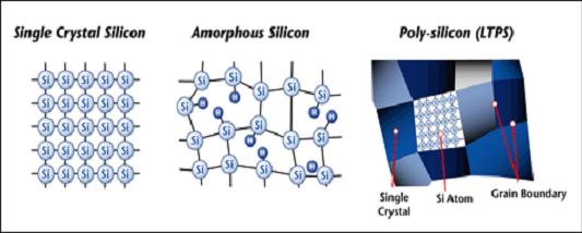
The technology for growing TFTs on glass substrates can be an amorphous silicon (a-Si) process and a low temperature poly-silicon (LTPS) process. The biggest difference between LTPS TFT and a-Si TFT lies in its The difference between electrical properties and the simplification of the process. LTPS TFT has a higher carrier mobility. Higher carrier mobility means that TFT can provide more sufficient current, but its manufacturing process is more complicated; while a-Si TFT is the opposite, although a-Si Sub-mobility is not as good as LTPS, but because of its relatively simple and mature manufacturing process, it has a better competitive advantage in cost. Looking at the companies that develop active OLEDs in the world, only AU Optronics can successfully combine OLEDs with LTPS and a-Si TFTs at the same time, becoming the leader in active OLED technology
Low temperature polysilicon
What is LTPS?
Polysilicon (polysilicon) is a silicon-based material with a size of about 0.1 to several um, which is composed of many silicon particles. In the semiconductor manufacturing industry, polysilicon is usually processed by LPCVD (Low Pressure Chemical Vapor Deposition), and then an annealing process higher than 900C, this method is SPC (Solid Phase Crystallization). However, this method is not suitable for the flat panel display manufacturing industry, because the maximum temperature of glass is only 650C. Therefore, LTPS technology is particularly applied to the manufacture of flat panel displays.
There are many ways to make LTPS films on glass or plastic substrates:
1. Metal Induced Crystallization (MIC): One of the SPC methods. However, compared with traditional SPC, this method can produce polysilicon at a lower temperature (about 500 ~ 600 C). This is because the thin layer of metal is coated before the crystal is formed, and the metal component plays an active role in reducing the crystallization.
2. Cat-CVD: A method for directly depositing poly-film without steam extraction. The deposition temperature can be below 300C. The growth mechanism includes the catalytic cracking reaction of the SiH4-H2 mixture.
3. Laser anneal: This is the most widely used method at present. Excimer laser is the main power, used to heat and melt a-Si, contains low amount of hydrogen components and then recrystallized into poly-film.
There are many ways to make LTPS films on glass or plastic substrates:
The production of LTPS film is much more complicated than a-Si, however, LTPS TFT is a hundred times more flexible than a-Si TFT. And can carry out CMOS procedure directly on the glass substrate. Listed below are several characteristics of p-Si that are superior to a-Si:
1. The mobility of the thin film transistor is faster, so the driving circuit can be directly made on the glass substrate, thus reducing the cost.
2. Vehicle for OLED: High mobility means it can provide larger drive current for OLED Device, so it is more suitable as a substrate for active OLED display.
3. Tight module: Since part of the driving circuit can be made on the glass substrate, the circuit on the PCB is relatively simple, which can save the area of ​​the PCB.
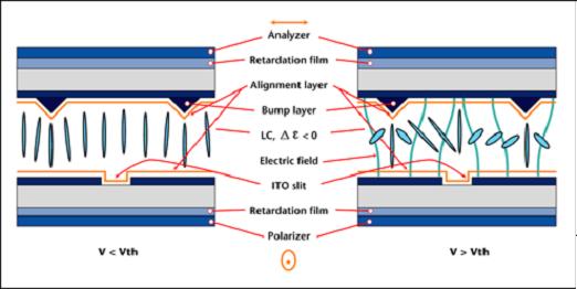
MVA
Due to the special arrangement mode of liquid crystal, MVA technology not only improves the viewing angle of the panel but also solves most of the grayscale inversion problems.
The advantages of using MVA technology are:
l High contrast
l Wide viewing angle
l No grayscale reversal
l High resolution
l Fast response time
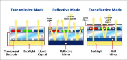
Transflective
The LCD screen is projected through the color filter through the backlight, and then reflected into our eye window. This mode with backlight is called "transmissive". Most of the power of the LCD screen is consumed by the backlight device . The brighter the backlight, the higher the brightness presented in front of the screen, but the greater the power consumption.
The "reflective" architecture uses an external light source to display the picture through the device of the reflective plate. This device saves power but the picture is more difficult to see in the absence of an external light source.
"Semi-transmissive and semi-reflective" is a compromise between the two. This device uses a half mirror to replace the reflective plate. In addition to the backlight, it can also use the reflection of the external light source to achieve power saving, improve brightness and The effect of reducing weight.
Different from the traditional process: COG technology assumes the driver IC directly on the glass substrate. The advantages of this technology include:
l Increasing packaging density and reducing weight makes the panel more thin and light
l Reduce the use of materials and reduce production costs
l Improve panel resolution

The ODF process is an epoch-making manufacturing method. In the past, it was time-consuming, low yield and difficult to achieve; such as the production of large-panel TV products, small Gap panels that respond to rapid response, or advanced high-quality MVA panels, using ODF process technology , The problem can be solved easily.
A simple comparison between the traditional process and the ODF process is as follows:

Using the ODF process, the advantages we can get from them are:
1. Decrease in machine investment: With ODF process, we no longer need vacuum tempering process, liquid crystal injection machine, sealing machine and panel cleaning equipment after sealing.
2. Space and manpower saving: Due to the reduction of the process described in item 1, relative manpower and space can be saved.
3. Material saving: Generally speaking, in the ODF process, the use efficiency of liquid crystal is more than 95%, but compared with 60% of the traditional process, it can save more than 35% of the liquid crystal material cost. It can also save the water, electricity, gas and lotion required for cleaning the sealing glue and related panels.
4. Reduced manufacturing time: Because the saved process is originally the most protracted and time-consuming process in the traditional process, and with the trend of large-scale panels, or small Cell Gap high-quality panels, the time consumption takes longer. The Cell process usually requires at least three days to complete in traditional practice, but for the ODF process, it can be completed in less than one day.
FTTH Cabling Accessories we here means the little insignificant parts but they are indispensable conditions when we do FTTH cabling .With quality level we required same as the fiber optic products, we use good quality plastic and stainless steel to make our ftth cabling accessories. Such like heat shrink tube splicing sleeves, conduit box, draw hooks, bending angle, cable clips, and so on.
With these FTTH cabling accessories, it is just like to put a coat on the fibers when you lay them in the wall corner or through the wall holes. The fibers is easily broken during pulling, torsioning and impacting. Besides, the dust cover can keep the fiber away from the dust that the fiber can work with good performance. It is a must to use such FTTH cabling accessories to ensure a qualified fiber play an important role in transmission.
FTTH Cabling Accessories, we also called FTTH Drop Cable Accessories,FTTH Structured Cabling Accessories(Tail Duct,Finishing Groove,Bending Angle, Kok Yin Angle, Hose Connector, Wall Tube,Wall Cable Tube, Plywood Retractors, Hole Wiring Duct,Seal Hole Trough, Hole Wiring Duct,Seal Hole Trough,S Type Fasteners,Dead-End Clamp,). we here means the little insignificant parts but they are indispensable conditions when we do FTTH cabling .With quality level we required same as the fiber optic products, we use good quality plastic and stainless steel to make our FTTH Cabling Accessories. Such like heat shrink tube splicing sleeves, conduit box, draw hooks, bending angle, cable clips, and so on.
With these FTTH Cabling Accessories, it is just like to put a coat on the fibers when you lay them in the wall corner or through the wall holes. The fibers is easily broken during pulling, torsioning and impacting. Besides, the dust cover can keep the fiber away from the dust that the fiber can work with good performance. It is a must to use such FTTH Cabling Accessories to ensure a qualified fiber play an important role in transmission.
We can also offer you:Fastening Hook, Hinger Support, Clamp Nail Buckle,Cable Clip, Clamp Nail Buckle, Fiber Cabling Metal Draw Hooks,Cable Hook,FTTH Clamp Retractor Hinger Support,Cable Manage Ring,Fiber Cabling Manage Ring,FTTH Drop Cable Management Ring.

FTTH Cabling Accessories
Fiber Optic Terminal Boxes, 24 port Rack Mount Fiber Enclosure, Sliding Rack Mount Fiber Patch Panel, SMC Terminal Cabinet, FTTH Products
NINGBO YULIANG TELECOM MUNICATIONS EQUIPMENT CO.,LTD. , https://www.yltelecom.com