Design of power amplifier in digital TV transmitter
Abstract: Using the latest LDMOS FET device, using a balanced amplifier circuit structure? Smoke power amplifier design in digital TV transmitters. The working frequency band is 470MHz ~ 860MHz, the gain in the whole frequency band is about 12dB, working in the linear state, the intermodulation suppression is less than -35dB.
Power amplifier is an important part of digital TV transmitter. Under normal circumstances, the signal in the digital TV transmitter is modulated by the COFDM method to output the intermediate frequency analog signal, which is sent to the amplification part through up conversion. The modulation method includes IFFT (8M) and IFFT (2M) two modes, consisting of 6817 and 1705 carriers respectively. The frequency interval between each carrier is very close, so the intermodulation signal easily falls within the frequency band, causing intermodulation distortion. Digital TV transmitters have higher requirements on linearity and stability than traditional types. The power amplifier in the transmitter is required to work in a higher linear state with stable gain.
The amplification part of the transmission system is divided into excitation and main amplification circuit. Among them, the excitation part is a broadband power amplifier. In order to ensure the normal and stable transmission of terrestrial digital TV, it needs to have good stability and reliability. Its working frequency band is 470MHz ~ 860MHz, and the working state is class AB; it requires a gain greater than 10dB, and intermodulation suppression Less than -35dB, the noise power density is greater than 130dB / Hz. This article uses the latest LDMOS FET device, and a balanced amplifier circuit structure? Smoke-driven design of digital TV transmitter driver stage power amplifier, after optimization and debugging, to meet system requirements.
1 Power amplifier design
1.1 Amplifier chip selection of power amplifier
This article uses Motorola LDMOS FET device MRF373 as the amplifier chip. Compared with BJT devices, the chip has a great improvement in linearity, gain and output capability, which greatly improves the reliability and maintainability of the transmitter. Compared with the traditional decimeter wave bipolar power amplifier tube, LDMOS FET has the following significant advantages:
· Can work under the condition of high standing wave ratio (VSWR = 10: 1);
· High gain (typical value 13dB);
· Saturation curve is smooth, which is conducive to analog and digital TV RF signal amplification;
· Can withstand large overdrive power, especially suitable for multi-carrier signals modulated by COFDM in DVB-T;
· The bias circuit is simple, no complex active low impedance bias circuit with positive temperature compensation is needed.
The LDMOS manufacturing process combines BPT and gallium arsenide processes. Unlike the standard MOS process, LDMOS does not use the BeO beryllium oxide isolation layer on the device package, but is directly hard-connected to the substrate, the thermal conductivity is improved, the device's high temperature resistance is improved, and the device life is greatly extended . Due to the negative temperature effect of the LDMOS tube, its leakage current is automatically shared when heated, instead of the positive temperature effect of the bipolar tube, which will locally form a hot spot in the collector current, so the tube is not easy to damage. Therefore, the LDMOS tube greatly strengthens the ability to withstand load mismatch and over-excitation. Also due to the automatic current sharing effect of the LDMOS tube, its input-output characteristic curve bends slowly at the 1dB compression point (saturation section used by large signals), so the dynamic range becomes wider, which is beneficial to analog and digital TV RF signal amplification. LDMOS is approximately linear when amplifying small signals, and there is almost no intermodulation distortion, which greatly simplifies the correction circuit. The DC gate current of the MOS device is almost zero, the bias circuit is simple, and no complex active low impedance bias circuit with positive temperature compensation is needed.
1.2 Circuit structure selection and comparison
Small-signal S-parameters can be used in the design of Class A amplifiers, which means that the amplification of the signal is basically limited to the linear region of the transistor. However, when it comes to high-power amplifiers, since the amplifiers operate in a non-linear region, small signals are usually nearly ineffective. At this time, the large signal S parameter or impedance of the transistor must be obtained to obtain a reasonable design effect.
Generally speaking, the distortion coefficient of Class A working state is the smallest and has good linearity. However, in the case of high-power applications, it is not applicable due to the low efficiency (50%) of the Class A working state. Adopt the circuit form of the class A and class B push-pull amplifier, can get the linear index similar to the class A amplifier.
The push-pull circuit is composed of two independent single-tube amplifiers without any internal connection, and the vector distribution and synthesis of power are performed through two baluns. Because the balun itself has the characteristics of variable resistance, the difficulty of impedance matching caused by the variable resistance ratio is greatly reduced, and the balun has a good suppression effect on even harmonics. However, because the distance between the two sides of the balun is too small, the two channels affect each other greatly, so the stability of the amplifier using the balun structure is poor, and the input and output standing waves of the circuit are relatively poor.
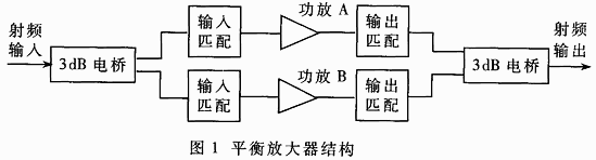
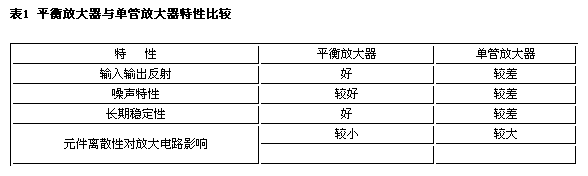
This article uses the form of balanced amplifier, the structure is shown in Figure 1. Its working principle is similar to the circuit of the balun structure, but due to the application of the 3dB bridge, the isolation between the two RF signals is better, which is conducive to the matching of the two ports. Compared with the single-tube amplifier structure, its advantages are shown in Table 1.
1.3 Matching network design
Since MRF373 does not provide internal matching, it is necessary to build a matching network in the amplifier circuit. The amplifying circuit in the digital TV reflection system works at 470MHz ~ 860MHz, and impedance matching needs to be achieved in a wide frequency band. The basic idea of ​​broadband amplifier matching circuit design is to use a reactance matching network to perform multi-level impedance transformation between the input and output of the amplifier and between stages. The network only plays a matching role, without extra power loss, can ensure the maximum transmission coefficient, balance the device characteristics, and can meet the bandwidth requirements of the system.
The load RL can be determined using the device's IV curve or through parameters such as output power and operating voltage. In order to maximize the output power, use RL to represent the internal drain load of the device as the target of the output matching circuit. If a network has the best match for a complex impedance, the output impedance of the network is equal to the complex conjugate value of the load impedance. The current load impedance is a pure real RL, so the best output matching circuit reflects the impedance of the device's drain load is the complex conjugate value of RL, namely:
RL = (VDD-VDS (sat)) 2 / 2P
Among them VDD is the working voltage, VDS (sat) is the inflection point voltage, P is the output power.
According to the above formula, the RL of MRF373 is about 6Ω.
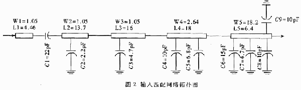
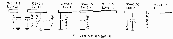
The amplifying circuit in this paper adopts the method of mixing separate components and distributed parameter components. Because inductance has a higher heat loss than capacitance, inductance is generally avoided in such circuits, and high-impedance transmission lines are used instead. A mixed-type matching network usually includes several transmission lines connected in series and parallel capacitors arranged at intervals. The input matching part of the amplifier adopts four-section continuous impedance transformation, and the output matching adopts a five-section continuous impedance transformation hybrid circuit. The input and output matching network topology diagrams are shown in Figures 2 and 3.
2 Circuit optimization and simulation results
Since the digital TV transmission system requires that the amplifier circuit must work in a linear amplification state, it can be analyzed by the small signal S-parameter method. With the help of small-signal S-parameter files provided by device manufacturers, ADS can be used to simulate small-signal S-parameters of the entire circuit to obtain small-signal gain, port matching, isolation and stability factor K. Table 2 shows the S parameters of MRF373 under (Vce = 26V, Ic = 500mA).
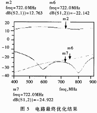
Circuit simulation with ADS does not meet the design requirements, and circuit optimization needs to be performed on this basis. When designing a power amplifier with only small-signal S-parameters as a model, the steps of circuit optimization are generally as follows: first, as much as possible, with RL (load resistance relative to maximum output power) matching as the goal, optimize and determine the output matching circuit component value; and then Optimize the component value of the input matching circuit, improve the gain and input matching circuit. It should be noted that before optimization, the output circuit model must be as complete as possible, and then optimized at the operating frequency to achieve the best match with RL. Figure 4 shows the simulation results of the amplifier circuit, and Figure 5 shows the final optimization results of the circuit.
3 Test results
After a lot of experiments and repeated debugging, the measured results are shown in Figure 6. The driver stage amplifier works in a linear state. It can be seen from the gain curve in Figure 6 that the gain in the entire frequency band is flat, about 12dB, which is roughly the same as the simulation result. The return loss is less than 15 dB, and the in-band standing wave ratio is less than 1.3. When the input power is 2 watt-hours, the output power is measured with a power meter of 25W, the signal amplitude is stable, and its intermodulation suppression is less than -35dB. Each index meets the system requirements, is close to the index of the amplifier in the similar digital TV transmitters abroad, and the cost is greatly reduced, which lays the foundation for the future development of localization of digital TV transmitters.
 Mind excerpt editor
Antenna design for mobile receiving terrestrial digital TV
1. Receive digital TV on the move, because the signal changes with different geographic locations, and the channel characteristics are dynamically changed, which requires the antenna to reflect the stability and reliability of the dynamic characteristics of different channels in real time. A certain bandwidth and gain must be guaranteed in all directions. To this end, we have designed an omnidirectional cylindrical spiral microstrip antenna, which spirally wound a quarter-wavelength microstrip resonator on a hollow cylinder with a certain thickness (h), and its microstrip patch It forms a coaxial cylinder with the floor, the volume is relatively short, it can be conformed with any carrier (such as an automobile), and it can be designed to be connected to a coaxial cable of any specification (50Ω, 75Ω), no matching network is required, and the hollow core can be Install active electronic devices.
The choice of a medium with a certain thickness (h) is to increase the radiation conductance so that the Qr value corresponding to the radiation and the total QT value decrease, thereby increasing the bandwidth. When the dielectric substrate is selected, the dielectric constant εr and the loss tangent tan δ are given at the same time. When εr is reduced, the medium's "bound" of the field is reduced. At this time, the antenna is easy to radiate, but relative to The energy storage of the antenna is reduced, the Qr value is decreased, and the frequency band is widened, but the reduction of εr will increase the size of the dielectric substrate. A large loss tangent can be selected to widen the Qr decreased frequency band, but the antenna efficiency is A lot of reduction, so it is necessary to consider as a whole. ?
Because εr and tanδ are functions of frequency, the actual measurement should be carried out after selecting the dielectric substrate, so as to avoid deviations in the position of the design feed point and affect the impedance matching. The dielectric material we choose is polytetrafluoroethylene (PTFE), which is stamped and formed at a time according to the designed size, and then the strip line and the floor are plated by the evaporation and ion copper plating process. ?
2. How to determine the microstrip bandwidth W?
Because the length of the strip line λg / 4 is related to εe (equivalent dielectric constant, λg = λ0 / εe), when εr and h are known, W depends on εe, which can be calculated according to the following formula: W = C * fr (εr + 12) ï¼12 ??
In the formula,? Fr——working frequency;
? C-speed of light;?
? εr-relative dielectric constant. ?
Digital TV generally works in the range of 470-860MHz, the bandwidth is 6-8MHz, and the gain is about 4dB. When the width less than the calculated by the above formula is selected, the antenna efficiency will be reduced. When the width is greater than the above formula, although the efficiency is higher, it is easy to produce high-order modes that affect the clarity of the image. In order to avoid complicated calculations in engineering, when designing microstrip lines, for the characteristic impedance of striplines of different media and different sizes, you can refer to the W / h, εe, and Z0 values ​​given in the microstrip antenna engineering manual. ?
3. Amendment to the spiral microstrip line?
Because the terminal of the spiral microstrip line is open, we theoretically think that the terminal open circuit has an infinite open circuit load impedance. In fact, it is not a real open circuit. There is an edge effect of the electric field at the open terminal, which is equivalent to adding a For the terminal capacitance, in order to counteract the influence of this terminal capacitance, the open end should be shorter than the ideal design calculation by a length of Δl. Because the terminal load impedance is infinite λg / 4, the input impedance of the transmission line is zero. When the terminal load is connected with an additional capacitor, if the input impedance is still to be kept at zero, the microstrip line will be shortened by a length of Δl. ?
Because the λg / 4 microstrip line is spirally wound on the cylinder, and a mutation (pointing) occurs at the end, this mutation will introduce additional reactance, so the microstrip line should be corrected for this mutation to offset this The effect of this kind of reactance. ?
The Δl value removed by its correction value is related to the values ​​of W, h, εr, and the use of microstrip correction theory analysis and calculation to introduce many complex functions is extremely complicated, and at the same time gives many assumptions, it is not easy to get accurate results. In actual work, it needs to be corrected through repeated experiments and accumulated experience. Δl is generally 0.2 times of the microstrip line. ?
The λg / 4 spiral patch antenna we designed eliminates the terminal capacitance by cutting off an angle of the microstrip line, and adds the effect of reactance. At the same time, it can also fine-tune the resonance frequency. When T1 is cut off, the frequency will increase, which will affect the impedance. Matching has little effect. When T2 is cut off, the frequency is also reduced, but it has a great influence on the impedance and needs to be readjusted, so it is more advantageous to consider the resonance operating frequency slightly lower when designing. In order to make the spiral microstrip antenna easy to radiate and receive, a certain distance of radiation gap (B) is left in the edge zone. Experience has shown that when the spatial separation between the two bands (S) is at least half the width of the microstrip (W), the antenna works best, so the number of spiral turns can be determined simply. To ensure the omnidirectional pattern, the width of the microstrip is not Should be smaller than the diameter of the cylinder (D). The feeding method directly affects the radiation characteristics of the microstrip line. We choose a 50Ω BNC type connector, back-feeding the output, the center line of the plug is connected to the feeding point of the microstrip line, and the grounding end is connected to the inner wall of the cylinder. In order to prevent the spiral microstrip line from being affected by the external environment, a glass cover is added outside the spiral patch microstrip antenna to prevent rain and snow. Add a magnet at the bottom of the antenna to attract the top of the car.
4 Conclusion?
China's development of digital TV started late, but the development speed is very fast, the market is particularly large, but it lacks its own proprietary technical standards. Although Tsinghua is developing a digital multimedia broadcasting terrestrial (DMB-T) standard, Jiaotong University is also developing advanced digital TV The terrestrial broadcasting (ADTB-T) standards are still being improved, and China must have its own independent intellectual property standards. At present, domestic manufacturers have the ability to provide DVB core equipment recognized by industry insiders, and have also launched many pilot programs of digital TV channels. Therefore, it is hoped that relevant departments will announce China ’s own terrestrial digital video broadcasting standards as soon as possible to create better digital TV. The environment allows people to enjoy high-definition digital TV programs brought by high technology.
heat film for clothes mainly keep people warm,we have used in Infrared Heating Jacket,Flexible Heating Flim for ski suit,Heating Flim For Diving Suit ,PET heaters film for heated clothes,Infrared Heater Type and New Condition PET heaters film for heated clothes,polyimide film heating element for Shoes,clothes,gloves,hand warmer,etc.we are a professional and leader Chinese exporter of heat film,Customization options (for example: SMT components, flex cable and connectors) can provide the perfect complete solution that can significantly reduce assembly time and increase productivity.Providing a variety of complex shapes design, and different power designs. Membrane in the same piece electrically heated heating circuit can be designed and holding circuit,we are looking forward to your cooperation.
Heat Film For Clothes Accessories
Heat Film For Clothes Accessories,Infrared Heating Jacket,Flexible Heating Flim,Heating Flim For Diving Suit
ShenZhen XingHongChang Electric CO., LTD. , https://www.xhc-heater.com