System design needs to consider many factors such as the RF link budget, antenna design, battery life, and RF adjustment circuit. In addition, it will involve a compromise between output power and transmitter current consumption. Maxim ’s low-cost transceiver chips (such as MAX1472 / MAX7044 / MAX1479 / MAX7030 / MAX7031 / MAX7032) integrate a unique power amplifier, allowing users to reasonably control output power and transmitter current consumption while ensuring high efficiency. This compromise Control is the key to improving battery life. Maxim devices do not need to modify the circuit when choosing between output power and common consumption, but simply change the load impedance of the power amplifier.
The following analyzes different types of power amplifiers, and gives the simulation results of Maxim transceiver chips.
Power amplifier type
Class A, B and C power amplifiers
The signal of the Class A power amplifier has a bias point. When the input signal amplitude changes, the average current consumed by the device does not change. In Figure 1, M1 can be seen as a current source with an amplitude of IDC.
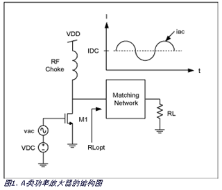
The output impedance corresponding to the maximum output power of the amplifier is: 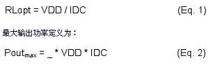
Therefore, the maximum efficiency of Class A power amplifiers is 50% [1]. It is assumed that while the bias current is guaranteed to be IDC, the drain voltage swing of M1 can reach the ground potential at the lowest. Working in the linear resistance area will reduce the actual efficiency of the Class A CMOS power amplifier to below 40%. This means that after the operating voltage is determined, in order to maintain high efficiency, the bias current of the class A power amplifier must change with the output power. Since the offset point of the class A power amplifier does not change with the change of the input signal, this type of power amplifier is the best structure in applications that pay attention to the linearity of the gain.
Compared with Class A, Class B and C power amplifiers can achieve higher efficiency, but usually have lower output power and greater distortion.
The common feature of Class A, Class B, and Class C power amplifiers is that active devices are treated as voltage-controlled current sources, and they are not expected to operate in a linear resistance region.
Class D, E and F power amplifiers
Contrary to Class A, Class B and Class C power amplifiers, Class D, Class E and Class F CMOS power amplifiers optimize efficiency and output power by operating in a linear resistance region. These power amplifiers are often referred to as "switch mode" power amplifiers. Because these power amplifiers can achieve high efficiency at low operating voltages, they are widely used in transceivers in the ISM band. As shown in Figure 2, in a switch-mode power amplifier, the output stage circuit is driven by a large-signal square wave.
The output stage transistor can be regarded as a resistor that performs switching operation according to the set frequency and duty cycle. It can also be seen from Figure 2 that the output stage transistors are rich in harmonic components. These harmonic components depend on the duty cycle and amplitude of the drive signal, the on-resistance of the field effect tube and the load resistance of the power amplifier. In class D power amplifiers, the output power is changed by changing the duty cycle of the input signal, which is the pulse width modulation mode (PWM). Class D power amplifiers are commonly used in the audio field where the output power varies continuously.
For Class E power amplifiers, the duty cycle of the input signal is constant. The matching network is used to minimize the drain voltage when the output stage switch is turned on. By minimizing the conduction voltage drop of the output stage switch, the loss of the switch tube can be reduced and the overall efficiency of the PA can be improved.
Class F power amplifiers are similar to class E power amplifiers, but special attention must be paid to harmonic impedance when designing matching networks to achieve the highest efficiency. Because of the need to consider harmonic resistance, the design of a Class F power amplifier matching network is generally more complicated.
Switch mode power amplifier
All Maxim's CMOS ISM band transceivers provide open-drain amplifier output. In the entire 300MHz to 450MHz frequency band, the duty cycle is fixed at 25%. The user designs the matching network according to the required output power, current loss and harmonic parameters.
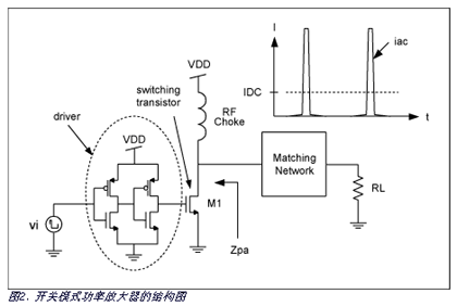
Figure 3 is a simple model of the output stage of a switch-mode power amplifier.
In the figure, Rsw is the on-resistance of the field effect tube, Cpa is the sum of the equivalent device parasitic capacitance, Cpkg is the package capacitance, and Cboard is the on-board capacitance. Table 1 lists the switch resistance and capacitance values ​​of the main transceiver devices in the Maxim ISM band.
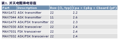
Note: The typical value of the on-resistance of the switch corresponds to the operating voltage of VDD = 2.7V; in addition, the parasitic capacitance on the board is greatly affected by the wiring. The design of class E and class F power amplifiers and matching networks can refer to literature [2, 3, 4], and readers can use these materials as a technical background. Considering the length of this article, only two points can be mentioned here: first, the design of the matching network must maximize the efficiency of the power amplifier; second, when the on-voltage drop of the output stage is low, the efficiency of the power amplifier is the highest.
Simulation of switch mode power amplifier
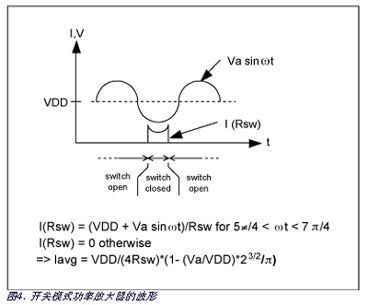
In many low-cost ISM band applications, system engineers may not be able to optimize the matching network due to the limitations of design cycle, cost, and system complexity. Small size (high Q value), inexpensive antennas usually have higher efficiency when transmitting higher frequencies, but the radio frequency adjustment circuit limits the harmonic content of the transmitted signal. Therefore, the suppression of harmonic components by the matching network is particularly important. Taking these factors into consideration, we assume that the output matching network has been optimized and the output voltage is a sinusoidal signal when analyzing the power amplifier. As shown in Figure 4.
Assuming that the load resistance of the power amplifier is RL, the output voltage can be as low as 0.1V, and the efficiency of the power amplifier is expressed as: 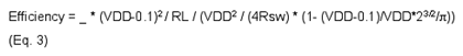
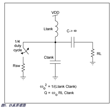
If the power supply voltage VDD = 3V, the switch on-resistance Rsw = 22Ω, the load resistance RL = 400Ω, the efficiency of the power amplifier is 80%, and the output power is 10.2dBm. Of course, the voltage waveform, switch on-resistance, and load resistance are all related, and the above formula does not accurately calculate the efficiency. SPICE can be used to build an ideal model of a switch-mode power amplifier, with an ideal resistance of 11Ω or 22Ω connected to a parallel resonant cavity with a Q value of 10. Figure 5 is the simulation principle diagram, and Figure 6 is the simulation result.
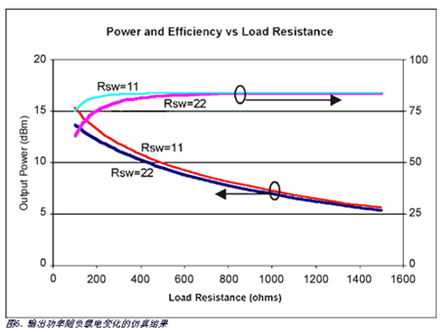
As shown in Figure 6, one of the most significant advantages of the switch-mode power amplifier is that while ensuring excellent DC-RF conversion efficiency, by changing the load resistance, the output power can be changed in a wide range. In addition, a switch-mode power amplifier with a smaller switch on-resistance has a larger output power and a higher efficiency. The disadvantage of a power amplifier with a lower switch on-resistance is that a larger current is required to charge and discharge the parasitic capacitance of the switching device.
As mentioned above, in order to improve efficiency, the switching amplifier must be turned on near the minimum voltage. In a simple parallel resonant circuit driven by a switched resistor, to achieve maximum efficiency, the imaginary part of the apparent load of the power amplifier at the operating frequency must be minimized (including parasitic capacitance of components, packaging and parasitic capacitance on the printed circuit board ). If the network is detuned, the efficiency of the power amplifier will decrease significantly. Figure 7 illustrates the results after the matching network is detuned when Q = 10 and Q = 5. 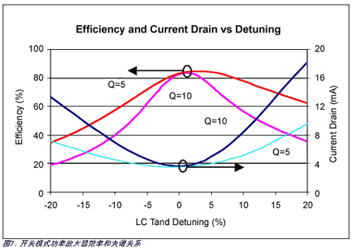
As shown in Figure 7, the minimum value of the drain current occurs at the resonance frequency. This fact can be used to verify whether the existing matching network has been optimized for a specific operating frequency. At the same time, it should be noted that SPICE simulation assumes that the opening and closing of the switch resistance are completed instantaneously; during the opening and closing of the switch, the parasitic capacitance of the switch does not change; the resonance inductance and capacitance have no parasitic impedance. The influence of these aspects makes the performance of the actual switch mode power amplifier lower than the ideal level. In special applications, iterative methods are usually used to optimize the matching network.
in conclusion
In summary, the important features of Maxim's switch-mode power amplifier in the ISM band are:
Switching power amplifiers optimize the efficiency and output power at low operating voltage by operating in a linear resistance region. This is different from Class A, Class B and Class C power amplifiers.
All Maxim's CMOS ISM band switch mode power amplifiers provide open-drain output. The user designs the matching network according to the required output power, current consumption and harmonic parameters. This flexibility allows users to adjust RF power and current consumption while ensuring high efficiency.
In order to maximize the efficiency of the switch-mode power amplifier, the switch must be turned on when the drain voltage is the lowest. To achieve maximum efficiency, the imaginary part of the load (including the parasitic capacitance of the component) of the switch-mode power amplifier at the operating frequency must be minimized , Package and board parasitic capacitance).
Depending on the load of the power amplifier, the minimum value of the drain current will appear at the resonance frequency. This fact can be used to verify whether the existing matching network has been optimized for a specific operating frequency and load
Aquarium Lamp,Aquarium Bulb,T8 Coral Tube,T8 Coral Bulb
Changxing leboom lighting product CO.Ltd. , https://www.leboomuv.com