Use configurable processors to create multi-standard multi-resolution video engines
With the rapid development of consumer electronics products, especially mobile phones, PDAs and portable media players (PMP), its requirements for terminal silicon suppliers have also greatly increased. For these vendors, designing ICs that can only be applied to one or two multimedia codecs or wireless standards is no longer enough. Consumers want their devices to play a variety of media using different encoding standards and wireless download standards. Therefore, a new and more flexible approach must be adopted to better adapt to the new media standards. In this article, we mainly talk about the challenges and opportunities faced by video decoders and encoder engines.
Design Method of Traditional Video Engine Based on RTL
The purpose of the previous-generation video ASIC design is to decode and encode MPEG-2, because this is the standard used by DVDs. Some of them also support MPEG-1, which can play VCD. In most cases, the logic implementation strategy of this single application is to use RTL (register conversion layer, register conversion logic) to design a customized MPEG-2 decoder and encoder. Figure 1 below is a typical MPEG-2 video ASIC structure, showing the RTL function block composed of the video subsystem, the main controller and the on-chip memory.
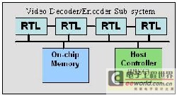
Figure 1: Typical MPEG-2 video ASIC structure
As the market situation changes, the current video ASIC must be able to support multiple video standards and have multiple resolutions. The traditional RTL method is no longer effective for the following reasons:
· As the number of standards increases, the number and complexity of RTL function blocks also increase;
Whether it is to implement a new video standard, upgrade existing existing standards, or modify bugs, silicon chip re-engineering is required;
In the 4-5 years after the implementation of the first generation of silicon, video codecs, especially encoders, have greatly improved in performance (bit rate, performance). To implement these improvements, silicon chips must also be reworked in all RTL methods.
Use a processor in the video engine instead of a fixed RTL
So, is there any other way? Using a programmable processor is the best solution, because it can solve all the problems mentioned above: (1) It is easy to establish a connection port between the processor and the codec; (whether it is a new video standard or an upgrade Existing codecs or bug fixes can be easily implemented in the software); (3) Through software upgrades, improvements in the implementation of video codecs can be easily applied.
However, due to its performance bottlenecks, traditional processors can only be used for general encoding, but not for video engines. Embedded DSP is not designed for video, but has the hardware functional units, instructions and interfaces required for general DSP applications. Therefore, to perform video encoding and decoding on traditional RISC and DSP processors means that these processors must run at very high speeds (MHz), and also require a lot of memory and consume a lot of power, but in portable devices, This obviously does not work.
As long as we make a simple analysis of the number of calculations required in a certain video kernel, it is easy to get this. The absolute error sum is an important calculation step performed in the motion estimation of most video decoding operations. The purpose of the SAD operation is to find the movement of the macroblock between two consecutive video frames. It does this by calculating the sum of the absolute errors between the corresponding pixel values ​​in each set of these two macroblocks.
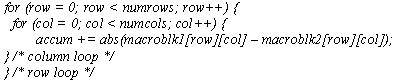
The following C code shows a simple execution of SAD operation:
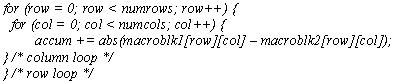
Figure 2 shows the basic calculation steps in the SAD operation. As shown in the figure, the main calculations are subtraction, absolute value calculation and result accumulation.
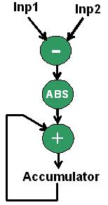
Figure 2: The main calculations performed in the absolute error sum (SAD) kernel
Calculating the SAD of two 16x16 macro modules on a RISC requires 256 subtractions, 256 absolute values, and 256 additions-a total of 768 calculations are performed, not including the load and memory required to transfer data. Since all macro modules in each frame must perform this operation, it is obvious that this is computationally expensive, and will become more and more difficult as the resolution of the video frame increases.
In fact, on a mid-range general-purpose RISC processor with instructions such as multiply and multiply-accumulate, if you want to perform H at CIF resolution. 26? Baseline decoding requires a rate of 250MHz, and if H is performed. 26? Baseline coding, the required rate is more than 1GHz. This means that the processor core alone consumes nearly 500mW of power, not to mention the power consumed by other parts of the memory and video on-chip system. Obviously, such a processor cannot be used as an embedded multimedia processor in portable devices.
Configurable processor solves the problem
How to perform SAD operation in the processor? One method is to write an instruction that can perform "subtract-absolute value-add" calculations at the same time. This can reduce the number of calculations required for the 16x16 macroblock from 768 to 256. In addition, since a functional unit that performs such integrated simple operations can generally be optimized into one cycle, it means that the calculation cycle is also reduced to 256.
But how to execute this "subtract-absolute value-add" instruction?
At this time, a configurable processor is required. The configurable processor is embedded, and the designer can choose from the configuration options menu and extend the processor functions by adding special application instructions, register files, and interfaces.
The following are some of the configurable and expandable features of current configurable processors. Traditional fixed processors do not have these functions:
Configurability, there are a series of options to choose from:
· Instructions that the designer wants or does not want, including: 16x16 multiplication or multiplication and accumulation, funnel conversion, floating point instructions, etc .;
Various functions such as zero consumption cycle, 5 or 7 stepping pipelines, the number of local data loading / storage units, etc .;
· Whether memory protection, memory conversion or a full memory management unit (MMU) is required;
· Whether a system bus interface is required;
· The width of the system bus and the local memory interface;
· The number and size of local memories;
· Number, type and level of interruption
Extensibility, you can freely add the following components customized by the designer:
· Registers and register files;
· Multi-period, arbitrarily complex functional units;
· SIMD functional unit;
· Convert the basic processor into a multi-launch processor;
· Customize interfaces that can read and write directly from the data path, such as GPIO (General Purpose IO) ports or pins on the processor core, and external interfaces that can be used to connect with other logic or processor cores Set FIFO.
The advantage of configurability is that you can build a moderate-sized processor by selecting the functional options required by your application, and the advantage of scalability is that designers can create instructions and registers that can speed up the application. Files, functional units, and interfaces to customize the processor to fully match its video application. But it must be noted that only today's advanced configurable processors can provide designers with custom scalability.
Build a video engine with a configurable processor
Create functional units that can perform multiple calculations
This step is the content of SAD operation and accelerated SAD operation.
For a configurable processor, adding this comprehensive computing function is a piece of cake. It can add a new instruction named "sub.abs.acc (subtract-find absolute value-add)" to perform "subtract, find absolute value and add" operation. As shown in Figure 3.
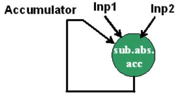
Figure 3: New instruction for "subtraction, absolute value and addition" operation
Modern configurable processors (such as Tensilica's Xtensa processors) are equipped with software tools that automatically modify editor tools, including C / C ++ editors, assemblers, debuggers, emulators, and ISS (instruction set simulators). At this time, the C editor will recognize the new C internal command "sub.abs.acc" and arrange the corresponding command, and the debugger will display sub. abs. The internal signal used in the acc function module, at the same time, the assembler will treat it as a new instruction, and the ISS will simulate it with cycle accuracy.
Create a new load / store interface
To read and write data in such a large register file (and corresponding SIMD functional unit), it is required to be able to load and store on a large scale. Still in a configurable processor, designers can customize load and store instructions to directly load and store data in custom register files. Then, the editor will automatically generate a load / store instruction corresponding to this load / store interface, so as to load the data from the memory into the register file.
FIG. 6 is an update diagram of the processor data path. As shown in the figure, the hardware generation tool automatically generates large custom register files and load / store interfaces as well as all relevant forward control and bypass logic. In particular, these tools also generate hardware logic to transfer data from the basic register file to the user-defined register file.
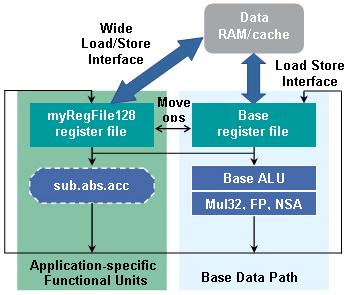
Image 6
Update address when loading or storing
When creating instructions for custom loading or storage, it is best to update the address while loading or storing. This new load / store instruction can be performed simultaneously:
Load A1 ↠memory (address 1); address 1 = address 1 + index change
This instruction, which can simultaneously perform data load / store and address update, allows the processor to perform back-to-back load / store without requiring an intermediary instruction to perform address update.
Create FIFO interface and general IO port
Another important feature of the configurable processor is the ability to define FIFO interfaces and general-purpose IO (GPIO) ports to read and write data directly from the data path. The width of these FIFO interfaces and GPIO ports can be arbitrary (1024b in this example), and there are no restrictions on the number (for example, the width of FIFO and GPIO ports can be 1024). These wide data path direct interfaces can provide the high data throughput required by multimedia and network applications to read, process, and write data through the processor core.
Figure 7 shows the data path with such a FIFO interface and GPIO port. (With this method) we can create an instruction to transmit two FIFOs (as long as they are not empty), perform a complex calculation (such as cyclic multiply-add), and pass the result to another output FIFO (As long as this FIFO is not yet full). Then, the hardware generation tool generates the appropriate interface signals, control logic and bypass logic again, and generates the complete RTL required by the configured processor. At the same time, the software generation tool automatically generates a complete set of editor tools and imitates Instruction cycle accuracy level ISS.
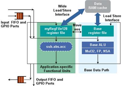
Figure 7: High-speed communication via FIFO interface and GPIO port
Speed ​​up complex control codes
The number and complexity of control codes in multimedia applications have increased to such an extent that it consumes almost as much computing time and work as the data-intensive part of the code. H. 26? A key part of the Mainprofile decoder-the CABAC algorithm (Content Adaptive Binary Arithmetic Coding) is such an example: this algorithm is almost a control flow decision tree, with a variety of complex data calculations and comparisons.
Because the calculation of CABAC is too complicated, many traditional processor solutions have to give up CABAC and choose a dedicated RTL accelerator. However, CABAC can function as a set of instruction extensions on the configurable processor. Not only does it have performance comparable to that of RTL solutions, but it also has another advantage over RTL accelerators, that is, its data does not need to enter and exit the processor . This shows another advantage of processor instruction expansion-because the special application hardware is located inside the processor, you can better separate the hardware and software.
to sum up
Modern configurable and scalable processors are the perfect choice for creating video and audio engines, and have been widely adopted by many semiconductor ASIC suppliers so far. There are also some video and audio IP products as embedded SoC modules. For example, Tensilica and its partners can provide a complete set of video and audio IP products, including XtensaHiFi2 audio engine and a series of multi-standard multi-resolution video solutions, and H. 26? (Basic, mainstream and advanced), MPEG-4 (SPandASP), MPEG-2, VC-1 / WM9 and various standard encoder and decoder software (codec). These video solutions cover QCIF, CIF, and SD, all aiming at achieving HD resolution, and starting point with low power consumption and small package.
As consumer demands expand the technical specifications of ASICs in consumer devices, more and more applications will be executed using configurable processors. With the help of the automatic design process brought by the configurable processor, the new function support will be as simple as the software upgrade, and the design and verification time will be greatly reduced.
PET Anti Blue Light Screen Protector
Pet Anti Blue Light Screen Protector,Ipad Screen Guard,Best Ipad Screen Protector,Anti Blue Light Ipad Screen Protector
Guangdong Magic Electronic Limited , https://www.magicmax.cc