1 Introduction
With the wide application of permanent magnet synchronous motors in various fields such as industry, agriculture and aerospace, permanent magnet synchronous motors have also been developed in the field of electric vehicle drive systems. As is known, permanent magnet synchronous motors operate stably and reliably, and position sensors need to be installed to detect position signals. Since the resolver (referred to as the resolver) can detect the rotor position of the motor by cooperating with the corresponding decoder chip, the resolver is widely used as a relatively reliable absolute position sensor. At present, many experts and scholars have begun to study the resolving position decoding system. With the continuous development of the revolving and decoding chip technology, the reliability of the revolving is higher and the decoding circuit is more compact. In this paper, the current latest generation of variable reluctance resolver and the decoding chip AD2S1205 are designed, and the corresponding resolver position decoding system is designed. The reliability of the system is verified by the test system.
2. The working principle of the revolution
The usual configuration of the resolver is that the primary winding is on the rotor and the two secondary windings are on the stator. There is no winding on the variable reluctance resolver rotor used in this system. As shown in Figure 1, the primary winding and the secondary winding are both located on the stator. This special design of the rotor allows the secondary coupling to follow the angular position. A sine change occurs as the change occurs.

Regardless of the configuration, the output voltage of the sinusoidal winding is S1-S3, and the output voltage of the cosine winding is S2-S4, as shown in equations (1) and (2). Where: θ is the shaft angle, ω is the rotor excitation angular frequency, and E0 is the rotor excitation amplitude.

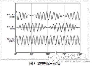
The variable reluctance resolver primary winding is excited by an AC reference source, and the two secondary windings are mechanically crossed by 90°. The magnitude of the voltage coupled across the secondary winding of the stator is a function of the angular position θ of the rotor relative to the stator. The rotational output signal is shown in Figure 2.
The principle of the converter tracking the shaft angle θ is that the converter produces an output angle φ and then feeds back φ to compare with the input angle θ. When the converter correctly tracks the input angle, the error between the two will be driven to zero. To measure the error, multiply (1) by cosφ, and (2) multiply sinφ by the difference:
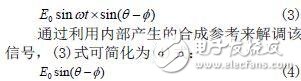
When the value of the angle error (θ-φ) is small, the equation (4) is approximately equal to 0E(θ-φ). The AD2S1205 features a closed-loop system of phase-sensitive demodulator, integrator, and compensation filter that seeks to zero the error signal. When this goal is achieved, the output angle φ is equal to the resolver angle θ within the rated accuracy of the converter.
3. Hardware circuit design
The design of the hardware circuit is developed around AD's decoding chip AD2S1205. First, the chip is a complete 12-bit resolution tracking resolver digitizer with a programmable sine wave oscillator that provides sinusoidal excitation for the resolver with an operating frequency range of 8.192MHz ± 25%. The chip uses a Type II tracking loop that can be used to track the input signal and convert the information at the sine and cosine inputs to the digital value corresponding to the angle and rate. The maximum tracking rate is a function of the external clock frequency. The Type II tracking loop continuously outputs position data with no conversion delay, and it provides noise rejection and harmonic distortion tolerance for reference and input signals.
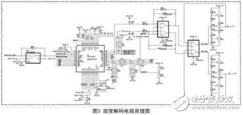
Figure 3 is a schematic diagram of a resolver decoding circuit. First, the differential sinusoidal excitation signal is generated by the AD2S1205 decoder chip. After the amplifier is amplified and followed, it is output to the motor by the push-pull method. The differential signals S1-S3 and S2-S4 returned by the motor revolving are processed by the IC26 and sent to the AD2S1205 for processing. The purpose of both SINLO and COSLO being connected to REFOUT is to enhance signal stability with a signal amplification of 1.5.
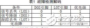
For fault detection, the chip has related fault detection functions. The priority level and fault code of the related faults are shown in Table 1.
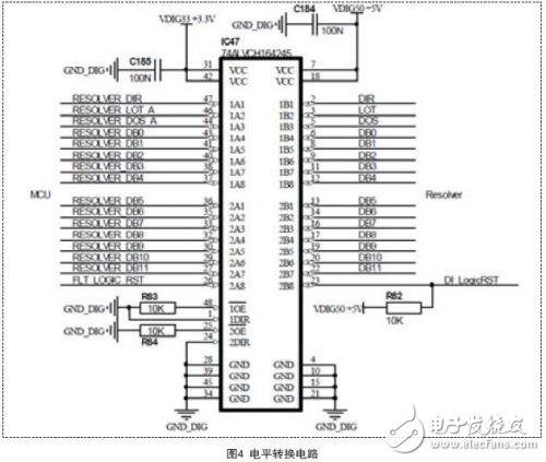
The level conversion chip adopts 74ALVCH164245. This chip converts the revolving signal into 3.3V and sends it to the MCU. The circuit is shown in Figure 4.
4. Software design
4.1 Reset Timing
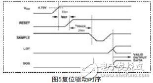
Figure 5 shows the AD2S1205 reset drive timing.
When the power supply voltage of the AD2S1205 is less than 4.5V, the AD2S1205 is in a low voltage reset state, and LOT/DOS is simultaneously low level indication, and there is no signal in the system reset. When the power supply voltage exceeds 4.5V, the RESET pin needs to maintain an active level of at least 10μs or more, which causes the AD2S1205 chip to be reset. After the reset is invalid, the AD2S1205 needs at least 20ms to make the internal circuit stable, and the tracking circuit can stably track the input angle. After a stable working time of 20ms, SAMPLE is valid and maintained for a period of time. The reset software flow is shown in Figure 6.

4.2 Parallel Port Data Read Timing
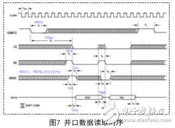
Figure 7 shows the drive timing for reading AD2S1205 data through the parallel interface. The parallel port data read timing starts from SAMPLE. SAMPLE must maintain 264ns valid time, latch internal angle/speed data into the angle/speed register, and then 750ns after SAMPLE is valid, the MCU can control the CS pin to be valid, allowing the latch to be enabled. And use the falling edge of RD to latch a value in the angle/speed register to the data pin (parallel mode). RDVEL determines whether the latch angle register or the speed register, so RDVEL must remain stable for the first 5 ns and the last 7 ns of the falling edge of RD. On the falling edge of RD, after 12ns delay, the angle data or speed data can be read from the parallel port.
5. Experimental results
The experimental test system consists of a test drive board, a resolver and a drag motor, as shown in Figure 8. The rotation of the motor drives the rotation to run on different rotation angles and rotation speeds. The excitation circuit outputs the excitation signal to drive the rotation, and simultaneously receives the feedback positive and cosine signals, and resolves the rotation angle and rotation speed of the rotation. By using the emulator, set the breakpoint control function debugging process before and after the initialization function, and observe whether the function running result is correct. Through the oscilloscope, observe whether the drive timing on the relevant pin after the function is running is correct, and observe the RESET/SAMPLE/LOT/DOS pin. During the initialization execution, it is necessary to refer to the reset timing to observe whether the RESET and SAMPLE pins controlled by the MCU send the corresponding level or pulse at the corresponding time. It is necessary to observe whether the DOS/LOT pin outputs high power if the system hardware connection is normal. Flat indication, or if the system hardware connection is not normal (such as the open circuit disconnection), whether the DOS/LOT pin outputs a corresponding fault signal after initialization.
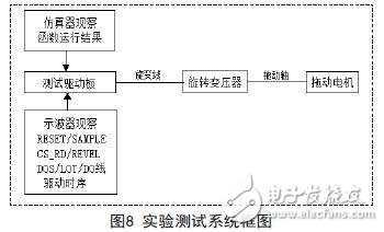
Figure 9 is a general diagram of the initialization function call of the AD2S1205.

Box a is the time point position at which to start the initialization function. At this time, the RESET pin sends a 15μs reset active low pulse, and simultaneously sets the SAMPLE/CS_RD two pins to the inactive high level. Box b is the point in time at which the initialization function ends. At this point in time, SAMPLE sends a 400 ns sampled active low pulse and then reads the DOS/LOT state supply layer. The overall time of the initialization function is 30ms, that is, the delay time from the end of the RESET reset to the SAMPLE effective reading of the DOS/LOT state is 30ms. The reading position test program calls the angle function and the velocity function every 100 μs. The test results are shown in Fig. 10.
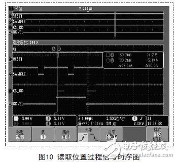
In Figure 10, SAMPLE valid time is 427ns; SAMPLE invalid time to read angle/speed delay is 750ns; RDVEL pin selects read angle/speed delay is 90ns; CS_RD valid time is 480ns, which basically reflects the decrease from CS_RD The delay time from the read angle/speed, CS_RD is invalid until the next read time is 200ns.
Therefore, the read angle function of the resulting AD2S1205 is tested to match its drive timing. The read speed function of the AD2S1205 obtained by the test is in accordance with its driving timing. Through the simulator verification, the angle value and speed value read by the test program are also in line with expectations.
6 Conclusion
Based on the principle and characteristics of the resolver and its decoding chip, this paper proposes a design scheme of the resolver position decoding system. The test results show that the hardware and software design of the scheme meet the motor position decoding requirements, and the timing is correct.
Maskking Disposable Vape is hot popular so far, like Mexico, Russia, and USA. It has many models so far, also coming more item in near future.
Maskking Vape,Maskking Gt-S Vape Device,Masking Gt-S Disposable Vape,E-Cigarette Maskking Gt Pod Device
Shenzhen Uscool Technology Co., Ltd , https://www.uscoolvape.com