Vision measurement technology is an emerging technology based on machine vision research, focusing on the measurement of the geometric dimensions of objects and the position and attitude of objects. With the increase of detection nodes, the amount of data that the visual measurement system needs to process is also increasing, which puts higher requirements on the measurement speed of the visual measurement system. The single data processing chip and the sequential data processing method can not meet the current stage. Design requirements for high speed vision measurement systems. In recent years, the development of microelectronics and integrated circuit manufacturing technologies, especially the development of field programmable gate arrays (FPGAs) and digital signal processors (DSPs), has provided new solutions for the improvement of measurement speed in visual measurement systems. Ideas and methods. Designing a targeted, high-speed visual measurement system for different measurement targets is an inevitable trend in the development of visual measurement technology.
1 overall design
The main purpose of high-speed vision measurement system research is to measure the geometric size, position and attitude of space fast moving targets based on computer vision, and to realize fast and real-time tracking of moving targets based on the above parameters. For the characteristics of high-speed motion of the target, the system uses the LUPA1300 high-speed CMOS image sensor produced by Fillfactory as the image acquisition device of the moving target. The image data is output through 16 parallel output amplifiers at full resolution, and the data transmission amount is 590MPixels/ s. The discrete analog pixel data output by the image sensor needs to be converted by a high-speed A/D converter to become a digital signal that the image processing system can process. The image processing system extracts the image features of the measured moving object from a large amount of image data by performing image denoising, enhancement, edge detection, target extraction and the like on the image data, and transmits the data to the decision system or the computer through the interface circuit. . The decision system or computer generates control signals of the mechanical mechanism according to the characteristic data, controls the motion of the entire visual measurement system, and realizes tracking and detection of high-speed moving targets. In this paper, the image acquisition and data processing functions of high-speed vision measurement system are studied, and a multi-channel parallel high-speed vision measurement system is designed. The system adopts the system structure combining FPGA and multi-DSP parallel processing, making full use of the characteristics of FPGA and DSP in operation speed and data processing, and realizes fast and real-time data processing function for a large amount of image data. The system can meet the requirements of real-time, stable and high-speed processing of fast moving targets. The overall principle block diagram of the system is shown in Figure 1.
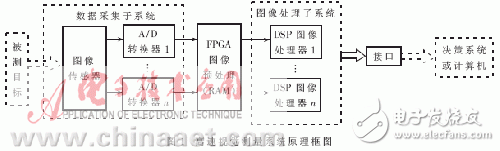
In the figure, the data acquisition subsystem uses low-voltage differential signaling (LVDS) technology to solve the impact of the walking line on circuit reliability and the limitation of transmission speed and distance. The image preprocessing subsystem with FPGA as the main function chip mainly realizes the functions of gray level correction, smooth denoising, image sharpening and the like for high speed image data, and also undertakes tasks such as bus control and frame storage control. The image processing subsystem based on the multi-DSP parallel processing structure mainly realizes the functions of edge detection, contour and position extraction of the target. The multi-DSP parallel processing structure connects a large-capacity SDRAM as a global external memory through a bus, and each DSP can also perform data transmission through a local bus, which is convenient for implementation of a pipelined or distributed parallel algorithm.
2 Design of data acquisition subsystem
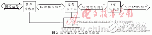
According to the characteristics of the high-speed motion of the target and the real-time requirements of the system design, the whole system must use high-speed image acquisition sensor and corresponding image amplification and A/D conversion circuit to realize real-time image acquisition and data conversion for high-speed moving targets. Figure 2 is a block diagram of the data acquisition subsystem.
2.1 LUPA1300 CMOS image sensor
At present, there are two main types of image sensors used in image acquisition: a CCD (Charge Coupled Device) image sensor and a CMOS (Complementary Metal Oxide Semiconductor) image sensor. Compared with CCD, CMOS image sensor has the advantages of low cost, low power consumption, single voltage, no smear, no halo, on-chip integration, etc., and its random read characteristics can be greatly improved in some cases. The rate of image acquisition [1]. Although the CMOS image sensor still has problems such as a slightly larger dark current in the ionization environment, high-resolution, high-performance devices to be further developed, with the development of solid-state image technology and integrated circuit technology, its application field will gradually expand.
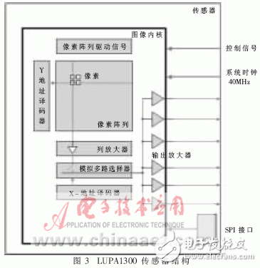
According to the above comparison and design requirements, the system decided to use the LUPA1300 high-speed CMOS black and white image sensor produced by Fillfactory as the image acquisition device for high-speed moving targets. The image sensor is a synchronous shutter active pixel sensor with 1 280&TImes; 1,024 pixel cell array, pixel size of 14 μm & TImes; 14 μm, frame rate of up to 450 frames per second at full resolution (open window) The frame rate can be higher). Its high frame rate is achieved by on-chip 16-channel parallel output amplifiers, each with a pixel rate of 40MHz, readout from left to right, and each output amplifier can drive a 10pF output capacitor. FIG. 3 is a structural schematic diagram of a LUPA1300 type CMOS image sensor.
2.2 A / D conversion circuit design
According to the image sensor's index, if each pixel is 10 bits, the image sensor will transmit 5.9 Gb/s (1 280&TImes; 1 024 & TImes; 450×10).
Data transmission or A/D conversion, if using the transmission mode of the walking line, will undoubtedly have a great impact on the reliability of the circuit, and the transmission speed and distance are also greatly limited, so that the current mainstream storage devices want to achieve this. Large data throughput is very difficult. Therefore, a new transmission method must be adopted during the transmission.
LVDS (Low Voltage Differential Signaling) is a low-amplitude differential signaling technique that uses a very low amplitude signal (approximately 350mV) to transmit data over a pair of differential PCB traces or balanced cables. It can transmit serial data at speeds of up to several thousand Mb/s [2]. LVDS has the advantages of high-speed transmission capability, low noise/low electromagnetic interference, low power consumption, etc. It has become the preferred signal form for high-speed I/O interfaces.
This paper selects Analog Devices' AD9212 chip as the data acquisition subsystem A/D conversion device. The AD9212 is an eight-channel LVDS serial A/D converter with a sampling accuracy of 10 bits, a maximum sampling frequency of 65 MS/s, and an analog bandwidth of up to 325 MHz. An on-chip sample-and-hold circuit is integrated. Two AD9212 chips can meet the data transmission speed and data volume requirements of the data acquisition subsystem. The AD9212 chip has special requirements for the input signal. In the design process, the analog differential amplifier AD8334 is used to amplify the analog signal output from the image sensor and then input it to the signal input terminal of the AD9212 chip. At the same time, the quality of the A/D converter clock has a significant impact on the signal acquisition, so a high-precision, low-jitter clock signal is required. In this paper, the clock driver chip AD9515 is used as the clock driver, and its ADC clock circuit is shown in Figure 4.

3 FPGA design for image preprocessing
Due to factors such as imaging conditions and noise, the image data after data acquisition contains a large amount of noise, which may cause the measured target image to be blurred relative to the entire image, so that the data processing part cannot be extracted from the image data. And dealing with the characteristics of the target being measured; at the same time, due to the light source and exposure time, the image data after data acquisition may have distortion phenomenon such as excessive distribution of gray scale or insufficient brightness of the whole image, which affects the detection accuracy and analysis result of the system. It is not conducive to the detection of the target, and may lead to detection failure in severe cases [3]. Therefore, before performing the feature extraction of the measured object, the system needs to send a large amount of image data to the image preprocessing subsystem for image grading correction, image smoothing denoising, image sharpening and other image preprocessing, so as to facilitate subsequent data processing. The subsystem is capable of quickly performing feature extraction and processing of the target being measured. The image preprocessing process needs to select an appropriate image preprocessing algorithm according to different measurement objects, in order to achieve fast grayscale correction, denoising and sharpening of the entire image sequence.
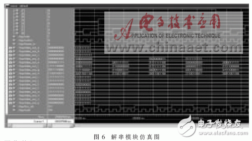
Most of the image preprocessing algorithms used by the image preprocessing subsystem are relatively simple, but the amount of data to be processed is large, and the data processing speed is required. Therefore, the FPGA chip is selected as the main function chip for image preprocessing, and each of its internal components The function of the module is shown in Figure 5. Figure 6 is a simulation diagram of the serial data deserialization module.

4 Image processing subsystem design of multi-DSP parallel structure
Image preprocessing only performs some simple processing on the image sequence, and does not extract the actual size, position, contour, attitude and other parameter information of the measured object. Therefore, the image data after image preprocessing must be sent to the image processing unit. Carry out further processing. Compared to the algorithm of the image preprocessing section, the algorithm of the image processing unit is more complicated and more difficult to implement. Because DSP is more suitable for complex algorithms, DSP chip is chosen as the main function chip of image processing. However, to achieve such a large amount of computation and high real-time requirements, the computing speed of a single-chip DSP seems to be inadequate. In this case, this paper uses multiple DSP parallel system structures instead of a single DSP chip to achieve image processing. In the actual design process, according to the computational complexity of the DSP algorithm and the real-time requirements of the system, this paper selects four DSP chips to jointly realize the processing tasks. The block diagram of the image processing section is shown in Fig. 7. In the figure, the FPGA is mainly responsible for timing control and frame data buffer control functions, and four DSP chips are used as data arithmetic processors to realize high-speed parallel processing of images. The entire image processing subsystem adopts a parallel processing structure combining a shared bus and two parallel structures based on the Link port. The data exchange between the FPGA and the DSP chip adopts a shared bus manner, and the data exchange between the DSP chips is performed by the DSP. The link port of the chip is implemented [4]. In this parallel bus mode, each DSP chip can independently implement its own algorithm program, or can perform parallel computing to jointly complete a DSP algorithm.
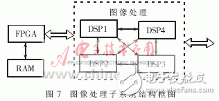
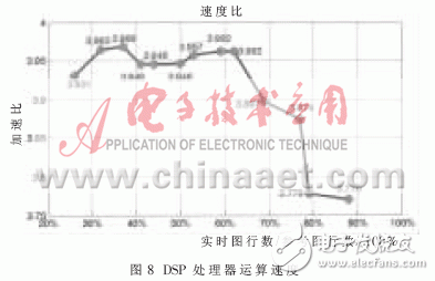
Figure 8 shows the speed comparison of four DSP data arithmetic processors with a single DSP data arithmetic processor. As can be seen from the figure, the speed ratio of the four DSP processors to the single DSP is between 3.770 and 3.969. In practical applications, the peak operation speed can meet the requirements of the image processing subsystem data processing.
In view of the characteristics of high-speed motion of the target and the real-time requirements of the vision measurement system, this paper focuses on the whole design and research process of high-speed vision measurement system, and proposes an image parallel processing structure based on FPGA and multi-DSP. According to the computing characteristics of FPGA and DSP, they are applied to the two systems of image preprocessing and image processing of high-speed visual measurement system respectively. Through experiments and tests, it is proved that this parallel processing structure can realize the processing function of high-speed visual measurement system. The working characteristics of the image acquisition device are also considered in the paper. The reliability and integration of the entire data acquisition part are greatly enhanced by LVDS technology, which facilitates the subsequent image processing functions.
Dc Axial Fan ,12V Axial Fan,Dc Axial Fan 12V,Dc Axial Fan 24V
Hangzhou Jinjiu Electric Appliance Co Ltd. , https://www.jinjiufanmotor.com