This system was originally designed for 8-channel QCM detection, that is, using 8 sets of identical oscillators with the MAX913 chip as the core, after being inverted by 2 CD4069 inverters, they are sent to the D end of 4 frequency differencers 74LS74, each There are 2 D flip-flops inside a difference 74LS74. Two 6M high-precision active crystal oscillators are converted into eight 6M output signals after passing through the clock chip CDCV304, and are sent to the CLK terminal of four frequency differencers 74LS74 respectively. The frequency signal after the difference of 74LS74 through 4 frequency difference devices is sent to the I / O port of the programmable logic device EPM570GT100C3 chip. EPM570GT100C3 is used here as a frequency meter, which is realized by software programming. The recorded difference frequency is sent to the 51 single-chip AT89S52 through the 8-bit data line. At the same time, the AT89S52 controls the EPM570GT100C3 to select which channel. The data processed by the AT89S52 is sent to the host computer through the 232 serial port.
The QCM coagulation sensor is a non-mass response sensor. It uses the high sensitivity of the quartz crystal oscillation frequency to the density and viscosity of the system where the crystal is located to detect the change of system properties. The QCM coagulation sensor detects the coagulation time and sedimentation rate of erythrocytes by the response of the sensor caused by changes in the impedance characteristics of erythrocytes. Therefore, using the biochip detection technology based on QCM sensor, a coagulation analyzer was developed.
Quartz crystal oscillation frequency is highly sensitive to changes in the crystal surface mass load (mass effect) and the physical properties of the reaction system such as density, viscosity, conductivity, etc. (non-mass effect). It has a sub-ng quality detection capability and its sensitivity can reach 1ng / Hz.
Taking a channel as an example to design a biochip detection circuit based on a QCM sensor, because a channel uses fewer logic gates, the programmable logic device EPM7128LC84-10 was selected. Figure 1 shows the overall design block diagram of the system.
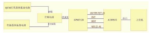
Figure 1 Overall block diagram of system design
hardware design
1. Quartz crystal oscillation and difference frequency circuit
In order to ensure that the QCM can oscillate after dropping the biological reagent, a special set of self-excited oscillator circuit must be used. The ordinary oscillator circuit composed of an inverter is not easy to start. The self-excited oscillator is usually basically amplified. It consists of three parts: circuit, positive feedback network and frequency selection network. In the quartz crystal oscillation circuit, the quartz crystal is the main component of the positive feedback network and is also a frequency selection network. The condition can only be met at the natural resonance frequency of the quartz crystal oscillator. According to this principle, an oscillator with the MAX913 chip as the core is used, and its output is a TTL level, which is convenient for signal acquisition of a single-chip computer or a programmable logic device. The square wave signal output from the QCM oscillator circuit for measurement is sent to the D terminal of the frequency difference device 74LS74. Refer to the square wave signal output from the high-precision 6M crystal oscillator to the CLK terminal of the frequency difference device 74LS74. The logic device counts, and the purpose of using the difference frequency is to reduce the frequency input to the programmable logic device EPM7128. Quartz crystal oscillation and difference frequency circuit as shown in Figure 2.
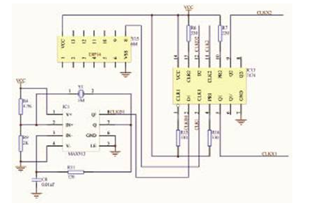
Figure 2 Quartz crystal oscillation and difference frequency circuit
2. Control circuit of EPM7128 and AT89S52
The difference frequency signal after the 74LS74 difference frequency converter is output from the 5-pin output of the 74LS74 to the 6-pin I / O port of the programmable logic device EPM7128. Because the pins of the programmable logic device are more flexible and have the ability to be erased and programmable, when modifying the original design, you only need to modify the original design file and then reprogram the programmable logic device chip without modification. The circuit layout does not need to reprocess the printed circuit board, which greatly improves the flexibility of the system and has a very good confidentiality. Here it is designed as a frequency meter through software programming. At the beginning of the measurement, the host computer sends a command to the 51 single-chip AT89S52 through the serial port. AT89S52 first sends a RST reset command to the 22 pin of EPM7128, so that the EPM7128 starts to work after the reset. Pin 46 sends an interrupt signal to the external interrupt 0 port (INT0) of AT89S52. After receiving the interrupt signal, the microcontroller sends three selection signals SEL0 ~ SEL2 to EPM7128 from P10 ~ P12 of P1 port. Because the 32-bit counter is designed in the EPM7128, and the 51 single-chip is an 8-bit machine, it needs 4 times to process the 32-bit data signal, which is controlled by the selection signals SEL0 ~ SEL2. Finally, 8-bit data signal is output from EPM7128 to the P0 data port of AT89S52. After being processed by the single-chip microcomputer, it is sent to the upper computer through the serial port for final data processing and graphic interface display. The hardware circuit diagram of this part is shown in Figure 3.
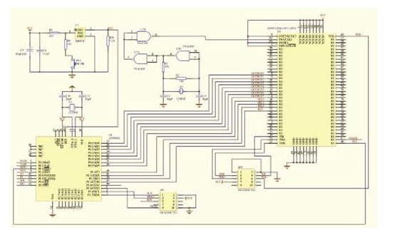
Figure 3 Programmable logic device EPM7128 and 51 single-chip AT89S52 control circuit
Pins 14 and 15 of AT89S52 are connected to crystal oscillator and capacitor to form a single-chip oscillator circuit. Pin 4 is the reset terminal and is controlled by IPM810. IPM810 has power-on reset, manual reset and undervoltage reset functions. AT89S52 uses PLCC44 pin packaged chip device, uses P1 port and reset port of single chip AT89S52 for online programming, and uses at89isp software for online programming to program the programming.
Pin 83 of EPM7128 is a global clock, which is a clock signal for external work. The clock signal can be generated using an active crystal oscillator or a passive crystal oscillator plus an oscillator. Pins 14, 71, 23, and 62 of EPM7128 are TDI, TDO, TMS, and TCK, respectively, and are JTAG programming ports. EPM7128 also uses online programming to program, using JTAG online programming. The other pins are basically I / O ports and can be specified as needed. In this design, the programmable logic device EPM7128 and the 51 single-chip AT89S52 are connected by a total of 13 wires for data communication and control. OUTPUT0 ~ OUTPUT7 are data communication, SEL0 ~ SEL2 are the chip selection control signals of AT89S52 to EPM7128, and INT is EPM7128 The interrupt control signal issued by AT89S52.
software design
In this system, the core program of ALTERA's programmable logic device EPM7128 is written in Verilog HDL hardware description language. It is compiled using MAX + plusII10.1 compilation system or Quartus II 4.2 compilation system. The design implements functions such as frequency division, frequency counting, and data selection. . 51 single-chip AT89S52 is mixed with C language and assembly language, and compiled with Keil C51 compilation system.
1. The top-level circuit of the programmable logic device EPM7128
The top-level circuit is shown in Figure 4, which is composed of a frequency division module, a counting module, and a data selection module. The frequency division module and the counting module are written in Verilog HDL hardware description language, and the data selection module uses a graphical input method. The 12M oscillation signal is sent to the CLK terminal of EPM7128, and after passing through the frequency dividing module, it becomes a frequency signal of 10Hz to provide the reference time base for the counting module. AT89S52 provides the reset RST signal to the RST end of EPM7128, resets EPM7128, and starts to record the frequency signal sent from the frequency differencer to the CLKX1 end of EPM7128. When the time is up, the output INT of EPM7128 sends out an interrupt signal to notify the microcontroller to receive data. Since the timer of the counting module is 32 bits, so through three 8-bit two-for-one data selectors, under the control of the SEL0 ~ SEL2 chip select signals given by the single chip microcomputer, time-out selects the output terminals OUTPUT7 ~ OUTPUT0 of EPM7128 The output 8-bit data signal to the P0 data port of AT89S52.
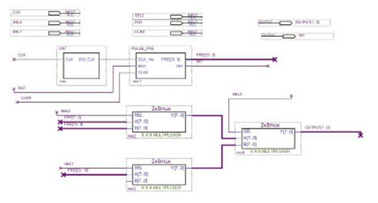
Figure 4 Top-level circuit of programmable logic device EPM7128
2. Frequency dividing module of programmable logic device EPM7128
The purpose of the frequency division module is to divide the 12M frequency signal input by the 83 pin of the programmable logic device EPM7128 into a 10Hz frequency signal to make the reference module as the reference clock, that is, the timing time is 100ms.
3. The counting module of the programmable logic device EPM7128 is sent to the counting module by the frequency-divided 10Hz signal from the frequency dividing module, which is added to the gate that can control the opening and closing time through the gate control circuit. The measured pulse is added to the input terminal of the gate in the counting module. When the frequency measurement starts, the counter is first set to 0. After the gate control signal arrives, the gate is opened to allow the pulse under test to pass, and the counter starts counting until the gate control signal ends. The gate closes and stops counting. Therefore, when the period of the gate control signal is 1s, the number of pulses measured through the gate at the gate opening time 1s is the frequency of the measured signal. In order for the host computer to obtain more data and accuracy, the gate control signal The period is 0.1s.
The following is part of the program code of the counting module of the programmable logic device EPM7128:
always @ (posedge CLK_1hz or negedge RST)
begin
if (! RST)
begin
CNT_EN = 0;
LOAD = 1;
end
else
begin
CNT_EN = ~ CNT_EN;
LOAD = ~ CNT_EN;
end
end
assign CNT_CLR = ~ (~ CLK_1hz & LOAD);
ssign INT = LOAD; // Use the rising edge of LOAD to interrupt the microcontroller.
always @ (posedge CLKX or negedge CNT_CLR)
begin
if (! CNT_CLR) // When CNT_CLR comes low, OUT = 0; the counter is cleared
OUT = 0;
else if (CNT_EN)
begin
OUT = OUT + 1; // When the rising edge of CLKX arrives, the counter is incremented by 1.
end end
always @ (posedge LOAD) // When the rising edge of the latch signal LOAD arrives, execute the following statement
begin
FRE = OUT; // Assign OUT to FRE
end
endmodule
The program key code of the counting module of the programmable logic device EPM7128 is given above. CLK_1hz represents the gate control signal, CLKX represents the measured pulse, RST is the system reset signal, FRE is the latched pulse frequency data, INT is the interrupt signal to the microcontroller, these signals are the input and output signals in the counting module. There are also several internally defined signals in the counting module. CNT_EN is the count enable signal, CNT_CLR is the count clear signal, LOAD indicates the latch signal, and OUT indicates the pulse frequency signal before latching. The gating signal is 10Hz, and the frequency measurement is performed every two clock cycles, that is, in every two clock cycles CLK_1hz, the CNT_CLR of the half clock cycle comes first, which is used for clearing; then, CNT_EN is valid for one clock cycle CLK_1hz To count; finally, in the next half clock cycle, when the rising edge of LOAD comes, the counting result is latched.
4. The program of 51 single chip AT89S52
The 51 single-chip microcomputer first initializes the timer, serial port and interrupt settings, etc., sends a reset signal to the EPM7128, and then enters the large-cycle program, waiting for an external interrupt. When the timing of EPM7128 is up, an interrupt signal is sent to external interrupt 0 of AT89S52, the program of AT89S52 jumps to the external interrupt, performs data processing, and gives a combination of selection signals SEL0 ~ SEL2 respectively. The serial port is sent to the host computer. Since the measured frequency will not exceed 10MHz, only 24-bit data can be read. Figure 5 is a flowchart of the external interrupt 0 interrupt program.
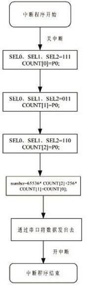
Figure 5 External interrupt 0 interrupt program flowchart
Experimental results
First add 100 microliters of plasma to the flow cell (warm bath 180S), rotate the screw to the scale of 17.0, and then inject the TT thrombin solution through the side hole and then withdraw the syringe. Figure 6 shows a 6mm diameter plasma coagulation experiment (plasma + TT thrombin = 100 + 100μl). This picture is the result of quartz crystal adopting AT tangent, silver electrode, base frequency I0MHZ, crystal diameter 6mm (no frequency difference is used), and directly send the frequency of 10MHz quartz crystal to programmable logic device for counting.
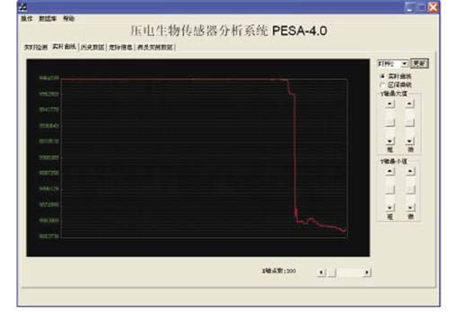
Figure 6 The plasma coagulation experiment with a diameter of 6 mm QCM as a micro-mass sensor has the advantages of simple structure, low cost, large vibration Q value, high sensitivity, and measurement accuracy of up to nanograms. It is widely used in chemistry, physics, biology, medicine And surface science. The piezoelectric quartz crystal sensor used in the detection of coagulation factors has the advantages of convenient use, high accuracy and low cost, and has broad clinical application and promotion prospects.
High Power Switching DC Power Supply
Switching Power Supply,Rack Mount Dc Power Supply,Programmable Dc Power Supply,Switching Mode Dc Power Supply
Yangzhou IdealTek Electronics Co., Ltd. , https://www.idealtekpower.com