Design and verification of an encrypted USB2.0 interface chip
0 Preface
The USB bus is popular among users because of its high speed, plug and play, and low power consumption. However, the USB specification itself does not consider the security issues during data transmission, so its low security performance is not suitable for transmitting information with high security requirements. In this paper, based on the study of the USB2.0 specification and the application of cryptography and other security protection technologies, an overall solution based on ASIC is proposed. The purpose is to use hardware description language to design a special integrated circuit that conforms to the USB2.0 specification and at the same time can automatically encrypt the data flowing through the interface chip. Finally, verify the designed system on FPGA, give the resources and performance parameters consumed by the system on FPGA, and analyze the obtained data.
1 Related knowledge
1.1 Introduction to USB
From the USB1.0 version to the 2.0 version, there have been many version updates in the middle. Beginning with Windows98 in July 1998, USB peripheral devices began to appear one after another, and also became the most popular interface. Its advantages are: easy to use, fast transmission, low price, low energy consumption, high stability, operating system Support, peripheral device support, and flexibility. The disadvantages are: lack of data security considerations, lack of support for old hardware, point-to-point communication, speed limitations, distance limitations, hardware errors or failures, and protocol complexity ,Copyright fee.
1.2 Introduction to AES
1.2.1 Principle and origin
AES (Advanced EncrypTIon Standard) was announced by the National Institute of Standards and Technology in 1997 to solicit the algorithm and finally selected two Belgian researchers Vincent Rijmen and Joan Daemen invented the Rijndael) algorithm, which was officially released in 2001. The AES standard was released.
1.2.2 AES workflow
The Rijndael algorithm is essentially a symmetric block cipher system. It uses a substitution / conversion network, and each round is composed of three layers: a linear mixed layer ensures a high degree of diffusion over multiple rounds; the nonlinear layer is confused by the juxtaposition of 16 S boxes The key encryption layer XORs the sub-key layer to an intermediate state. Rijndael is an iterative block cipher. Its block length and key length are both variable. Only in order to meet the requirements of AES, the processed packet size is limited to 128 bits. The key length is 128 bits, 192 bits, or 256 bits, and the corresponding number of iteration rounds Nr is 10 rounds, 12 rounds, and 14 rounds. Can resist powerful and real-time attacks.
2 System solutions
2.1 System principle
The main purpose of this article is to design a special integrated circuit design that not only complies with USB2.0 data reception and transmission, but also automatically encrypts the received data, and uses the FPGA to verify the function of the designed system.
The system consists of two major modules: USB module and AES encryption module. The system structure is shown in Figure 1:
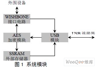
Among them, the USB module realizes that the flow-through data is received and sent according to the USB2.0 specification. Assemble and package the data to be sent, and decompose the received data packet. After the processing of the memory interface and the priority discrimination module, store the data in the external memory (SSRAM) or communicate with peripheral devices through the WISHBONE interface circuit ; The AES encryption module is responsible for encrypting the received data, and the key is encapsulated in the memory in the chip.
2.1.1 Principle of USB interface module
This module implements data processing in accordance with the USB2.0 specification and the interconnection and data communication between different peripherals and computers. The main functions of this module include:
(1) It fully supports the USB2.0 specification, provides full-speed mode and high-speed mode, and its data rates are 12Mbit / s and 480Mbit / s, respectively.
(2) Support the data communication between the WISHBONE interface circuit and the module by DMA.
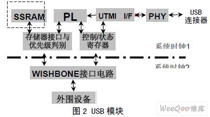
(3) Suspend / resume function of the module. The module structure is shown in Figure 2. among them. The PHY module is responsible for sending data to the computer connected to the USB connector, or receiving data from the computer; UTMI (Universal Data Transceiver Macrocell Interface) is connected to the PL (protocol layer) module and internal data storage, control registers to maintain communication data The format conforms to the protocol format in the USB2.0 specification; WISHBONE (main interface circuit) is a communication bridge between internal data storage, control registers and external devices.
2.1.2 Principle of AES module
This module is responsible for encrypting the data received and unpacked by the USB module and then storing the encrypted data in external memory or sending it to the peripheral device through the WISHBONE interface circuit.
The block diagram of this module is shown in Figure 3. It mainly includes data bit width conversion module and AES encryption unit. In the USB module, the data reception and processing bit width is 8, and in the AES encryption module, the plain text and the key bit width are 128, so the data obtained after unpacking the received data packet in the USB module cannot be directly encrypted. Encryption is only possible after bit width adjustment. The function of the data bit width conversion module is to connect the 8-bit data after PL unpacking into 128 bits, and then send them to the AES encryption unit; the AES encryption unit performs the ten rounds of AddRoundkey with the 128-bit plaintext and the key in the key memory. , SubBytes, ShiftRows, MixColumns complete the plaintext encryption after conversion, and send the encrypted data (ciphertext) to external memory or send it to the peripheral equipment through the WISHBONE interface circuit.

2.2 Performance analysis
This article uses the EP1S10F484C5 chip of the StraTIx series to verify the system.
2.2.1 Performance analysis of USB2.0 module
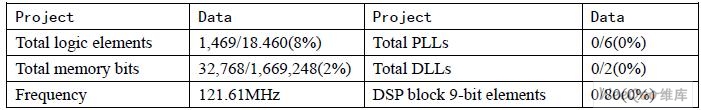
The following table shows the integrated performance parameters of the USB module:
2.2.2 Performance analysis of AES module
When the input information = {32 43 f6 a8 88 5a 30 8d 31 31 98 a2 e0 37 07 34}, the number of rounds Nr = 10, the encryption key = {2b 7e 15 16 28 ae d2 a6 ab f7 15 88 09 cf 4f 3c }, The encryption result = {39 25 84 1d 02 dc 09 fb dc 11 85 97 19 6a 0b 32}, and the result is verified to be correct, which fully complies with the AES encryption algorithm.
The following table is the combined data of AES encryption algorithm:
2.2.3 Performance analysis of the entire system
The following table shows the performance parameters after system synthesis:
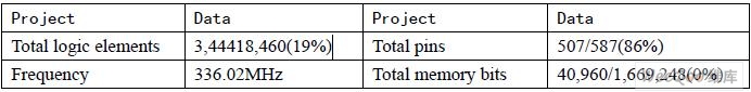
From the analysis of the above comprehensive results, it can be concluded that the verification of the system on FPGA is completely feasible, and its frequency can reach 336.02MHz, which can completely achieve the transmission speed of USB480Mbits / s.
2.3 Necessity and feasibility analysis of system implementation
The main purpose of the system is to design a USB2.0 interface chip that can automatically encrypt data. The conventional USB interface chip does not have encryption function. However, a large part of the USB application field today needs to encrypt the transmitted data. The security requirements are particularly high, so making a dedicated integrated circuit that conforms to the USB2.0 specification and can automatically encrypt data will have a large application space in the application. Making such an integrated circuit is necessary.
FPGA is a kind of reconfigurable hardware, which has both hardware security and high speed, as well as software flexibility and easy maintenance. It has become a hot research direction for hardware implementation of block cipher algorithms; in addition, FPGA development has a higher startup cost than ASIC To be small, the cycle from FPGA design to the market is very short, FPGA chip reconfiguration and expansion is very convenient, it can negotiate the required cryptographic algorithm, the replacement cryptographic algorithm can be configured to the target device in a timely manner. Currently, the capacity of FPGA chips continues to increase, and there is embedded memory on-chip, which makes it easy to implement lookup tables and conversion operations. Therefore, it is feasible to implement the system mentioned in this article in a million-gate FPGA.
3 System advantage analysis
Measures to improve the reliability of USB data communication can be basically divided into two types: one is to encrypt the data after being processed by computer software; the other is to directly encrypt the data at the hardware level. The software processing is relatively simple to implement, but the software encryption processing speed is much slower than the hardware encryption. If a large amount of data needs to be encrypted in real time, the software processing will consume too much time, which is not suitable for real-time data encryption and communication. On the contrary, if it is solved by hardware, it will obtain an ideal real-time encrypted communication effect in terms of speed.
In addition, due to the large number of complex bitwise operations used in encryption algorithms, and these types of operations are generally not suitable for running on general-purpose processors, the implementation of software will inevitably bring about inefficiencies, and the encryption chip architecture is Specially designed for the structural characteristics of encryption algorithms, using some special optimization techniques (such as pipelines and lookup tables, etc.), which can greatly increase data traffic and reduce key generation time; in addition, the software can only provide limited physical security , Especially in the storage of keys. The encryption algorithm and related key generation process are implemented in hardware and encapsulated in the chip, because they are not easy to be read or changed by external attackers, and will have higher physical security. Therefore, the hardware-based cryptographic algorithm has received widespread attention in the industry, and can be fully qualified for the security of the entire system.
From the above analysis, it can be seen that the system uses hardware to handle encryption and USB communication, which can greatly improve the security of the system on the basis of data transmission that meets the USB2.0 specification.
4 Conclusion
In summary, by studying the need for USB communication security, the development of a USB device controller with real-time automatic encryption of data can create a new field of USB secure communication, and now, most of the peripheral interfaces of devices on the market support USB, if you can develop a high-secrecy, simple and easy-to-use chip that does not affect the original USB communication, it will be favored by the majority of users.
Magnetic Starter is mainly applied to circuit of AC 50 or 60Hz,voltage up to 550V for far distance making and breaking circuit and frequent start and control motor. It has the features of small volume, light, weight, low power consumption, high efficiency, safe and reliable perfomance etc.
The types of Magnetic Starters are as following:
LC1-D Magnetic Starter
NEW Type Magnetic Starter
BLS-MB Magnetic Starter
Star-Delta Starter

Magnetic Starters
Magnetic Starter,Magnetic Motor Starter,3 Phase Motor Starter,3 Phase Magnetic Starter
Ningbo Bond Industrial Electric Co., Ltd. , https://www.bondelectro.com