Abstract: The MAXQ3180 microcontroller is a multiphase analog front end of an electric meter. It has all the functions of a modern multi-function meter. The MAXQ3180 transmits its reading to the host microcontroller via the serial peripheral interconnect (SPI â„¢) bus. This application note describes how to implement this interface and demonstrates example code to help designers implement this communication mechanism.
Introduction to SPI Serial Peripheral Interface (SPI) is a bus protocol between devices that enables fast, synchronous, full-duplex communication between chips. A master drives the synchronous clock and chooses which slaves to address. Each SPI peripheral contains a shift register and control circuit to enable the addressed serial peripheral interconnect SPI peripheral to be able to send and receive data simultaneously.
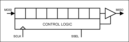
Figure 1. Schematic diagram of SPI slave
SPI communication uses four different circuits: SCLK: synchronous clock used by all devices. The master drives the clock, and the slave receives the clock. Note that SCLK can be gated and there is no need to drive between SPI operations. MOSI: Master comes out, slave comes in. This is the main data line that the master drives all slaves on the SPI bus. Only the selected slave synchronizes the data from MOSI. MISO: the master enters, the slave exits. This is the main data line driven when the selected slave sends to the master. Only the selected slave can drive this circuit. In fact, this is the only circuit in the SPI bus arrangement that allows slave drives. SSEL: This signal is different on each slave. When active (usually low), the selected slave must drive MISO. For this discussion, it is important to note that the SPI peripheral sends and receives at the same time. The simplest understanding is that the host always sends one byte and receives one byte.
Some SPI peripherals sacrifice speed to simulate half-duplex operation. The MAXQ3180 microcontroller does not use this method, it is a true full-duplex SPI slave.
The rest of this application note describes how to connect and successfully use the MAXQ3180 on the SPI bus.
Introduction to MAXQ3180 communication To the host, the MAXQ3180 looks like a memory array, containing both RAM and ROM. This is because the ROM firmware in the MAXQ3180 reads the operating parameters of the RAM and puts the results in the RAM. Therefore, configuring the MAXQ3180 is as simple as writing blocks to RAM.
Some MAXQ3180 “storage†locations trigger internal operations of the device and calculate the meter measurement results “at any timeâ€. Write "nop" to these locations. The discussion of the special functions and purposes of RAM and virtual ROM locations is beyond the scope of this document. The most important thing here is that the microcontroller does only have two SPI communication operations: read and write.
Each operation in the MAXQ3180 starts with the host sending two bytes, which contains the command (for example, read or write), the address to be accessed, and the number of bytes accessed. As mentioned earlier, each SPI peripheral returns one byte for each byte received. Therefore, MAXQ3180 returns 0xC1 after receiving the first command byte, and returns 0xC2 after the second command byte. This protocol is shown in Figure 2 below.
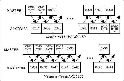
Figure 2. The host reads and writes data to the MAXQ3180
If the host reads one or more bytes, it must send null bytes. Remember, the master cannot receive any information from the slave, unless it sends some information: send a byte to get a byte. But after receiving a command, the MAXQ3180 calculates the result. When the host sends a null byte, it may not be ready. For this reason, the MAXQ3180 always sends multiple bytes (0x4E or ASCII 'N') such as zero or NAK characters before sending data, followed by an ACK character (0x41, or ASCII 'A').
If the host writes one or more bytes, it sends the data to be written immediately after sending the command. MAXQ3180 returns ACK (0x41) for each data byte. Then, it returns NAK (0x4E) until the write cycle is completed, and then returns the final ACK.
Note that after the final ACK, the MAXQ3180 is ready to start the next operation; it does not need to wait for anything else. It does not even need to trigger SSEL to start the next operation. MAXQ3180 knows that the first operation has been completed and is ready for the next operation.
For any reason, if you need to reset the communication between the host and the MAXQ3180 (for example, if the communication is asynchronous), the host only needs to wait 200ms before restarting the communication from the first command byte. The 200ms delay indicates MAXQ3180, the host gave up the previous operation.
Command byte Command byte tells MAXQ3180: The operation to be applied is READ or WRITE The length of the RAM address to change (or the virtual ROM address to be read)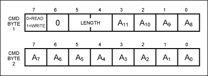
Figure 3. Command byte structure
The first command byte (Figure 3) tells MAXQ3180 whether the operation requested is READ or WRITE, and the length of the operation. The command byte structure is as follows:
The rest of command byte 1 and all command byte 2 provide the address of the RAM byte to be accessed (or the same virtual ROM function).
Host software design Although the MAXQ3180 contains a hardware SPI controller, the software program in the ROM firmware still has to process each message byte. For this reason, there is a delay between consecutive bytes. In the current MAXQ3180 model, this delay must not be less than 100µs to achieve reliable operation. Please refer to Figure 4 and Figure 5.
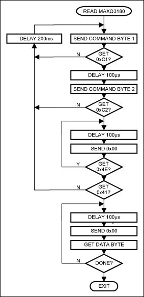
Figure 4. Flow chart for reading MAXQ3180
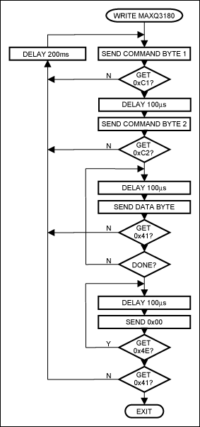
Figure 5. Flow chart for writing to MAXQ3180
The code list provides code to implement the interface of the MAXQ2000 microcontroller with the built-in SPI host and the MAXQ3180. Other microcontroller users need to provide their own SPI primitives and may also need to modify high-level subroutines.
In the following list, the dly_us subroutine stops the program thread from executing for a few microseconds. Define the SPI_TIMEOUT constant to provide a parameter that is longer than the character timeout.
In high-level subroutines, ENUM is used to select registers by name. Among other parameters, it provides the index of the register_lookup_table array, which contains the register length of each MAXQ3180 register. Please refer to Figure 6, Figure 7 and Figure 8.
Figure 6. Send_SPI source code
Figure 7. ReadAFE (SPI_Read) subroutine code
Figure 8. Write_AFE (SPI_Write) subroutine code
Introduction to SPI Serial Peripheral Interface (SPI) is a bus protocol between devices that enables fast, synchronous, full-duplex communication between chips. A master drives the synchronous clock and chooses which slaves to address. Each SPI peripheral contains a shift register and control circuit to enable the addressed serial peripheral interconnect SPI peripheral to be able to send and receive data simultaneously.
Figure 1. Schematic diagram of SPI slave
SPI communication uses four different circuits: SCLK: synchronous clock used by all devices. The master drives the clock, and the slave receives the clock. Note that SCLK can be gated and there is no need to drive between SPI operations. MOSI: Master comes out, slave comes in. This is the main data line that the master drives all slaves on the SPI bus. Only the selected slave synchronizes the data from MOSI. MISO: the master enters, the slave exits. This is the main data line driven when the selected slave sends to the master. Only the selected slave can drive this circuit. In fact, this is the only circuit in the SPI bus arrangement that allows slave drives. SSEL: This signal is different on each slave. When active (usually low), the selected slave must drive MISO. For this discussion, it is important to note that the SPI peripheral sends and receives at the same time. The simplest understanding is that the host always sends one byte and receives one byte.
Some SPI peripherals sacrifice speed to simulate half-duplex operation. The MAXQ3180 microcontroller does not use this method, it is a true full-duplex SPI slave.
The rest of this application note describes how to connect and successfully use the MAXQ3180 on the SPI bus.
Introduction to MAXQ3180 communication To the host, the MAXQ3180 looks like a memory array, containing both RAM and ROM. This is because the ROM firmware in the MAXQ3180 reads the operating parameters of the RAM and puts the results in the RAM. Therefore, configuring the MAXQ3180 is as simple as writing blocks to RAM.
Some MAXQ3180 “storage†locations trigger internal operations of the device and calculate the meter measurement results “at any timeâ€. Write "nop" to these locations. The discussion of the special functions and purposes of RAM and virtual ROM locations is beyond the scope of this document. The most important thing here is that the microcontroller does only have two SPI communication operations: read and write.
Each operation in the MAXQ3180 starts with the host sending two bytes, which contains the command (for example, read or write), the address to be accessed, and the number of bytes accessed. As mentioned earlier, each SPI peripheral returns one byte for each byte received. Therefore, MAXQ3180 returns 0xC1 after receiving the first command byte, and returns 0xC2 after the second command byte. This protocol is shown in Figure 2 below.
Figure 2. The host reads and writes data to the MAXQ3180
If the host reads one or more bytes, it must send null bytes. Remember, the master cannot receive any information from the slave, unless it sends some information: send a byte to get a byte. But after receiving a command, the MAXQ3180 calculates the result. When the host sends a null byte, it may not be ready. For this reason, the MAXQ3180 always sends multiple bytes (0x4E or ASCII 'N') such as zero or NAK characters before sending data, followed by an ACK character (0x41, or ASCII 'A').
If the host writes one or more bytes, it sends the data to be written immediately after sending the command. MAXQ3180 returns ACK (0x41) for each data byte. Then, it returns NAK (0x4E) until the write cycle is completed, and then returns the final ACK.
Note that after the final ACK, the MAXQ3180 is ready to start the next operation; it does not need to wait for anything else. It does not even need to trigger SSEL to start the next operation. MAXQ3180 knows that the first operation has been completed and is ready for the next operation.
For any reason, if you need to reset the communication between the host and the MAXQ3180 (for example, if the communication is asynchronous), the host only needs to wait 200ms before restarting the communication from the first command byte. The 200ms delay indicates MAXQ3180, the host gave up the previous operation.
Command byte Command byte tells MAXQ3180: The operation to be applied is READ or WRITE The length of the RAM address to change (or the virtual ROM address to be read)
Figure 3. Command byte structure
The first command byte (Figure 3) tells MAXQ3180 whether the operation requested is READ or WRITE, and the length of the operation. The command byte structure is as follows:
| Length Code | Data Length |
| 0b00 | 1 byte |
| 0b01 | 2 bytes |
| 0b10 | 4 bytes |
| 0b11 | 8 bytes |
The rest of command byte 1 and all command byte 2 provide the address of the RAM byte to be accessed (or the same virtual ROM function).
Host software design Although the MAXQ3180 contains a hardware SPI controller, the software program in the ROM firmware still has to process each message byte. For this reason, there is a delay between consecutive bytes. In the current MAXQ3180 model, this delay must not be less than 100µs to achieve reliable operation. Please refer to Figure 4 and Figure 5.
Figure 4. Flow chart for reading MAXQ3180
Figure 5. Flow chart for writing to MAXQ3180
The code list provides code to implement the interface of the MAXQ2000 microcontroller with the built-in SPI host and the MAXQ3180. Other microcontroller users need to provide their own SPI primitives and may also need to modify high-level subroutines.
In the following list, the dly_us subroutine stops the program thread from executing for a few microseconds. Define the SPI_TIMEOUT constant to provide a parameter that is longer than the character timeout.
In high-level subroutines, ENUM is used to select registers by name. Among other parameters, it provides the index of the register_lookup_table array, which contains the register length of each MAXQ3180 register. Please refer to Figure 6, Figure 7 and Figure 8.
| unsigned char Send_SPI (unsigned char x) {unsigned char y = 0; int z; int error = 0; SPICN = 3; / * MSTSM, SPIEN * / z = 0; while ((SPICN_bit.STBY) && (++ z <SPI_TIMEOUT)); if (z == SPI_TIMEOUT) error = 1; SPICN_bit.SPIC = 0; / * Clear transfer complete flag * / SPIB = x; z = 0; while ((! SPICN_bit.SPIC) && (++ z <SPI_TIMEOUT)); if (z == SPI_TIMEOUT) error = 1; y = SPIB; SPICN_bit.SPIC = 0; dly_us (100); if (error) return 0; return y;} |
| long Read_AFE (enum METER_REGISTER_RECORD reg, uint16 reg_addr) {extern unsigned char record [8]; unsigned long x = 0; unsigned char i, regadd, command_code = 0; for (i = 0; i <8; i ++) record [i ] = 0; switch (register_lookup_table [reg] .register_length) {case 2: command_code | = 0x10; break; case 4: command_code | = 0x20; break; case 8: command_code | = 0x30; break;} command_code | = reg_addr> > 8; regadd = reg_addr & 0xff; / * Disable SPI to reset it * / SPICN_bit.SPIEN = 0; for (x = 0; x <300; x ++); SPICN_bit.SPIEN = 1; SPI_SELECT_0; i = 0; while ((Send_SPI (command_code)! = 0xC1) && (++ i <SPI_COMMAND_RETRIES)) spi_comm_timeout (); x = 0xffffffff; if (i == SPI_COMMAND_RETRIES) goto spierror; Send_SPI (regadd); i = 0; while ((Send_SPI (0)! = 'A') && (++ i <SPI_RETRIES)); if (i == SPI_RETRIES) goto spierror; x = 0; for (i = 0; i |
| void Write_AFE (enum METER_REGISTER_RECORD reg, uint16 reg_addr, uint32 data) {uint8 i, regadd, command_code = 0x80; int x; switch (register_lookup_table [reg] .register_length) {case 2: command_code | = 0x10; break; case 4: command_code | = 0x20; break; case 8: command_code | = 0x30; break;} command_code | = reg_addr >> 8; regadd = reg_addr & 0xff; / * Disable SPI hardware to reset it * / SPICN_bit.SPIEN = 0; for (x = 0; x <300; x ++); SPICN_bit.SPIEN = 1; SPI_SELECT_0; i = 0; while ((Send_SPI (command_code)! = 0xC1) && (++ i <SPI_COMMAND_RETRIES)) spi_comm_timeout (); if (i = = SPI_COMMAND_RETRIES) goto spierror; Send_SPI (regadd); for (i = 0; i |
Digital Table Clock,Digital Clock,Nexie Tube Clock For Table,Table Clock Oak Wood
Guangzhou Huanyu Clocking Technologies Co., Ltd. , https://www.findclock.com