PCB board is the commonly known printed board. In our school, the printed board was turned into an electrical schematic, as a basic training and training, and named as a map. Proper identification of the PCB is a critical step in the repair process. For electronic technicians, there are many basic skills to master, and correct identification of electrical schematics and printed boards is an important part of this.
Due to the maturity of technology, PCB boards can be made into single-panel, double-panel, multi-layer boards, and the like. For us, the identification of multi-layer boards is difficult. Therefore, the map here mainly refers to the identification of single panel and double panel.
To this end, you should first understand the layout of the components, the functions of the components, and the division of the functions of the unit circuits. From the overall situation, analyze, grasp, and do some preparatory work.
1. Identify the unit circuit functions. In terms of identifying PCB printed boards, it is critical to understand what functions a unit circuit can perform. In the study of electrical principles, units that conform to certain functions can be represented by boxes. Therefore, in the map, the identification box is identified by the reverse analysis. For example, to identify whether the printed board is a color TV main board? Is it an electromagnetic cooker control board? Is it an energy-saving fluorescent light control board? Or a battery car charger control board? For example, it is said locally whether it is a single-tube amplifying circuit or a bridge-type rectifying circuit, whether it is a successful discharging circuit or a self-oscillating circuit.
2 recognize the type of chip or component on the PCB. After identifying the model of the chip, the reference map can be referenced against the typical application circuit diagram of the chip. For example, power amplifier block TDA2616; color TV decoding block LA76810; field scan integrated block LA7841; switching regulator power supply control block; single chip chip 89C2051 and so on. If the chip model read out has not been seen before, you can also check it online, read the typical application schematic diagram of its DATASHEET technical document on the Internet, and then compare the PCB board to draw the peripheral circuit component label of the chip. . The printed circuit board circuit of the chip can be quickly clarified.
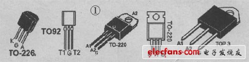
3. Usually master the packaging form of some components. Common packages include TO-92, TO-220, etc. The three legs of the triode are E, B, and C, respectively. The low-power plastic package is generally TO-92, and the recognition port is: "Upper and lower feet, from left to right E, B, C" (with some exceptions). The TO-220 plastic triode identification port is: "Look at the literal face down, from left to right B, C, E." The three legs of the FET are D, C, S. T0-220 plastic FET identification port is: "Look at the literal face down, from left to right C, D, S. The three sides of the thyristor are A, G, K, and the two-way is T1 (A1) , G, T2 (A2), pin and package corresponding situation as shown in Figure 1.
In addition, the core components should be grasped, and the power supply of the core components and the signal input and output should be used as a starting point for identifying the PCB to perform the map. Usually the core components are nothing more than triodes, FETs, thyristors and integrated circuit chips. These core components are active devices that require power to operate. Therefore, it is very important to find out the power and ground wiring reasonably. The high potential of the NPN transistor is the C pole, the PNP transistor is the E pole, and the high potential of the FET is generally the D pole. The thyristor high potential is A, and the integrated chip power supply pin can check the data. The ground wire is generally a copper foil with a relatively large area at the edge, and the ground wire at the middle position is often connected to the heat sink (also special, preferably measured by a multimeter electric barrier measurement). When analyzing the power supply, it should start from the high potential and go to the ground. In each power supply line, the highest potential, usually with a large filter capacitor, can be used as a basis for judgment. As for the input and output of the signal, it should be treated according to the common-amplifier circuit of the triode, the common-base amplifier circuit, and the common-amplifier circuit. The control of the FET and the thyristor is extremely G-polar, that is, the B-pole of the usual triode. The FET of the FET and the thyristor is the position of the small signal input, the C pole of the triode, and the D pole of the FET as the output position of the signal. The thyristor has no signal output. The input and output of the integrated circuit chip can be discriminated by referring to its technical documentation.
Galaxy S8 Snap3D Case is a 3D viewer in phone case shape, you can take it and watch 3D movies on your smartphone with this 3d viewer.
HOW TO USE THE SNAP3D Case AS A 3D SCREEN
The attached 3D screen on the Snap3D acts like 3D glasses.
To turn your smartphone into a 3D device, you need to first download the [Mplayer3D" application.
Then install the Snap3D on your smartphone screen and run Mplayer3D.
Enjoy the stunning stereoscopic 3D!
About Mplayer3D
An application that transforms your smartphone into a 3D TV.
Can be download for free.
Supports video streaming on YouTube
A video player which DOES NOT support contents.
Provides demo videos only in the download section.
Supported format: MP4
DOES NOT support 2D to 3D conversion.


Galaxy S8 Snap3D,Snap3D For Galaxy S8,Galaxy S8 Snap 3D Viewer,Galaxy S8 Snap3D Case
iSID Korea Co., Ltd , https://www.isidsnap3d.com