The design of FDLs is difficult due to technical constraints. At present, optical buffering can only be realized by using optical delay line groups, that is, a group of optical fibers of different lengths. Literature [1] proposed three different FDLs designs, as shown in Figure 2.
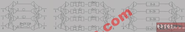 |
(a) FDLs design 1 (b) FDLs design 2 (c) FDLs design 3
Figure 2 FDLs design scheme In Figure 2a, the FDL cache is composed of N delay lines, each delay line provides a different delay time, but the delay provided by each delay line is fixed, the delay range is 0 to the maximum cache time B = (N-1) b, b is the delay time of a single delay unit (shown as a circle in the figure), and N is the series of FDLs.
The FDL cache shown in Figure 2b also has N delay lines, but the difference from Figure 2a is that the delay time provided by each delay line is not fixed and can vary from 0 to B, where B = (N-1) b = (20 + 21 +,…, + 2n) b. The rectangular box in the figure shows a 2: 2 cross unit. This structure is called "variable delay" FDL cache. The implementation of the fixed-delay FDL cache is simple, but the application is not flexible enough; the variable-delay FDL cache is relatively expensive (mainly proportional to the number of 2: 2 cross units).
The structure shown in FIG. 2c is a mixed structure of the above two structures. Each delay line provides variable delay, but the range of delay is different, the lower limit is 0, the upper limit is b, 2b, ..., (N-1) b.
As shown in Figure 3, due to the limitations of its own design, FDLs will have out-of-end conflict problems.
Figure 3a shows that two burst data packets have arrived on the same wavelength successively. When passing through FDLs, due to their different delays, they have collided at the exit of FDLs. Figure 3b shows that the arriving burst packet conflicts with the burst packet already buffered in the FDLs. The existence of this conflict will have a certain impact on the switching performance of the node. 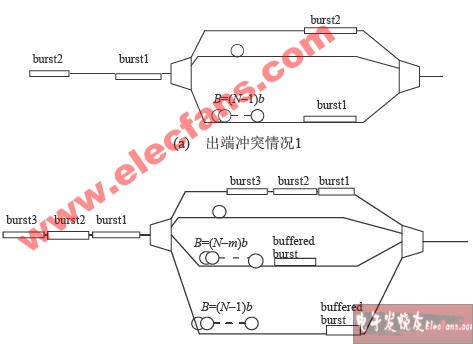
(b) Outbreak conflict 2
Figure 3 FDLs outgoing conflict Research on FDLs and TWC in OBS Exchange Structure |
The Description of GSM Magnetic Antenna
Gsm Magnetic Antenna Features :
Vehicle exterior antenna. Multi-band versatility.
Easy to install and use.
Lightweight and weatherproof.
Good quality. Keep it in place while traveling.
Simply transfer from one car to another.
More signal for your phone when you are driving.

The Specifications of GSM Magnetic Antenna
* Frequency range: 900-1800MHz.
* Bandwidth: 70/170MHz.
* Gain: 3 -5dBi.
* VSWR: ≤2.0.
* Input Impedance: 50Ω
* Maximum input power: 50W
*Wire length: 3M/Customized
* Input connector type: SMA Male/Customized.
*Operating temperature: -40~60ºC
*Polarization: Vertical
*Mounting way: Magnetic adsorption
GSM Magnetic Antenna
Gsm Magnetic Antenna,Magnetic Base Antenna,GSM Magnetic Base Antenna,Magnetic Car Antenna
Shenzhen Yetnorson Technology Co., Ltd. , http://www.yetnorson.com