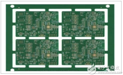
PCB (Printed Circuit Board), the Chinese name for printed circuit boards, also known as printed circuit boards, is an important electronic component, a support for electronic components, and a carrier for electrical connection of electronic components. Because it is made by electronic printing, it is called a "printing" circuit board.
After the electronic equipment adopts the printed board, due to the consistency of the same printed board, the manual wiring is avoided, and the electronic components can be automatically inserted or mounted, automatically soldered, and automatically detected to ensure the quality of the electronic equipment. Increase labor productivity, reduce costs, and facilitate maintenance.
PCB development history and origin
Printed boards have evolved from single layers to double-sided, multi-layer and flexible, and still maintain their respective trends. Due to the continuous development of high precision, high density and high reliability, the volume is reduced, the cost is reduced, and the performance is improved, so that the printed board still maintains a strong vitality in the development of electronic equipment in the future.
The domestic and international discussion on the future development trend of printed board manufacturing technology is basically the same, that is, high density, high precision, fine aperture, fine wire, fine pitch, high reliability, multi-layer, high-speed transmission, lightweight, The development of thin-type direction, at the same time, to improve productivity, reduce costs, reduce pollution, and adapt to the development of multi-variety and small-scale production. The technical development level of printed circuits is generally represented by the line width, aperture, and plate thickness/aperture ratio on the printed board.
The creator of the printed circuit board was the Austrian Paul Eisler. In 1936, he first used a printed circuit board on the radio. In 1943, Americans used the technology for military radio. In 1948, the United States officially recognized the invention for commercial use. Printed circuit boards have been widely used since the mid-1950s.
Prior to the advent of the PCB, the interconnection between the electronic components was done by direct connection of the wires. Today, wires are used only in laboratory applications; printed circuit boards are definitely in an absolute control position in the electronics industry.
PCB production process:
First, contact the manufacturer
First you need to contact the manufacturer, then register the customer number, then someone will quote you, place an order, and follow up the production schedule.

Second, the material
Purpose: According to the requirements of the engineering data MI, cut into small pieces on the large sheet that meets the requirements. Small pieces of sheet that meet customer requirements.
Process: large sheet material → cutting board according to MI requirements → seesaw → beer fillet \ edging → exit board
Third, drilling
Purpose: According to the engineering data, the required aperture is drilled at the corresponding position on the sheet of the required size.
Process: stacking pin → upper plate → drilling → lower plate → inspection \ repair
Fourth, sinking copper
2. Objective: The copper is deposited by chemically depositing a thin layer of copper on the walls of the insulating holes.
Process: rough grinding → hanging board → copper line automatic line → lower board → dip % dilute H2SO4 → thick copper
Five, graphics transfer
Purpose: Graphic transfer is the transfer of images on the production film to the board
Process: (blue oil process): grinding board → printing the first side → drying → printing the second side → drying → explosion → shadowing → inspection; (dry film process): hemp board → laminating → standing → right Bit → Exposure → Rest → Shadow → Check
Sixth, graphic plating
Purpose: Graphic plating is to electroplat a layer of copper on the exposed copper skin or hole wall to a desired thickness of copper layer and a desired thickness of gold or tin.
Process: upper plate → degreasing → water washing twice → micro-etching → water washing → pickling → copper plating → water washing → pickling → tin plating → water washing → lower plate
Seven, unwinding
2. Objective: Retreat the anti-plating coating layer with NaOH solution to expose the non-line copper layer.
Process: water film: inserting → soaking alkali → washing → scrubbing → passing machine; dry film: placing board → passing machine
Eight, etching
Purpose: Etching is the use of chemical reaction method to corrode the copper layer in non-line parts.
Nine, green oil
Purpose: Green oil transfers the pattern of green oil film to the board to protect the line and prevent tin on the line when soldering parts.
Process: grinding plate → printing photosensitive green oil → 锔 plate → exposure → shadow; grinding plate → printing the first side → baking sheet → printing the second side → baking sheet
Ten, characters
Purpose: Characters are provided as an easy-to-identify mark
Process: After the end of green oil → cool and cool → adjust the network → print characters → after 锔
Eleven, gold-plated fingers
Purpose: Plating a nickel/gold layer of the required thickness on the plug finger to make it more wear resistant
Process: upper plate → degreasing → water washing twice → micro-etching → water washing twice → pickling → copper plating → water washing → nickel plating → water washing → gold plating
Tin plate (a process of juxtaposition)
Purpose: Spray tin is sprayed with a layer of lead tin on the bare copper surface not covered with the solder resist oil to protect the copper surface from oxidation and oxidation to ensure good soldering performance.
Process: micro-etching → air drying → preheating → rosin coating → solder coating → hot air leveling → air cooling → washing and drying
Twelve, molding
Purpose: Through the die stamping or CNC machine to cut out the shape forming method required by customers, organic enamel, beer board, handcuffs, hand cut
Note: The accuracy of the data board and the beer board is higher, the handcuffs are second, and the hand cutting board can only make some simple shapes.
Thirteen, testing
Objective: Through the electronic 100% test, it can detect the open circuit, short circuit and other defects that are not easily found by visual observation.
Process: upper mold → release board → test → qualified → FQC visual inspection → unqualified → repair → return test → OK → REJ → scrap
Fourteen, final inspection
Purpose: Through 100% visual inspection of the appearance defects of the board, and repair of minor defects, to avoid problems and defective board outflow.
Specific work flow: incoming materials → view data → visual inspection → qualified → FQA random inspection → qualified → packaging → unqualified → processing → check OK
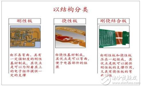
PCB structure classification and industry trends:
PCB is mainly composed of two kinds of materials: insulating substrate and conductor, which plays a role of support and interconnection in electronic equipment. Electronic components such as integrated circuits and resistors and capacitors cannot function as individuals. Only when they are supported by printed circuit boards and connected, they can perform their functions in the whole. Depending on the structure, number of layers, etc., the PCB can be classified as follows:
PCB classification by structure
PCB sorted by number of layers

The middle and lower reaches of the PCB industry are clearly defined. The upstream industry includes raw materials suppliers such as glass fiber, ink and copper cladding. The midstream industry includes PCB production equipment suppliers, and the downstream industry covers multiple application fields. The industrial chain can be divided into raw materials - copper clad laminate - printed circuit board - electronic product applications.
PCB industry chain
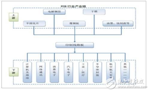
According to the use of downstream electronic products, PCB can be used in consumer electronics, automotive electronics, network communications, industrial control medical, aerospace and other fields. In the field of consumer electronics, PCBs are used in mobile phones, home appliances, drones, VR devices, etc.; in the automotive electronics field, PCBs are used in GPS navigation, car audio, car dashboards, automotive sensors, etc.; in the field of network communication PCB application In the optical module, filter, communication backplane, communication base station antenna and other equipment; in the industrial control medical field PCB used in industrial computers, inverters, measuring instruments, medical displays and other equipment; in the aerospace field PCB used in aircraft, aviation Remote sensing systems, aerial radars and other equipment.
The use of PCB in various downstream fields

After decades of development, the PCB industry has become a global industry, but in recent years the total capacity has shown a low-speed development trend. According to the China Merchants Research Institute, the global PCB market output value reached US$54.2 billion in 2016. Although it is 2% lower than the market output value in 2015, it is still the largest proportion of the electronic component segmentation industry. Driven by the continued development of the global electronic information industry, the global PCB market is expected to maintain a growth rate of around 2%.
Global PCB industry output value

China PCB industry output value

The industry is moving eastward, and the mainland is unique. The focus of the PCB industry is constantly shifting to the Asian region, and the production capacity in Asia has further shifted to the mainland, forming a new industrial structure. Before 2000, 70% of global PCB production value was distributed in Europe, America (mainly North America) and Japan. With the continuous transfer of production capacity, the PCB production value in Asia is now close to 90% of the global market, which is the dominant PCB in the world, and mainland China has become the region with the highest PCB production capacity in the world. At the same time, the production capacity in the Asian region has shown a trend of shifting from Japan, South Korea and Taiwan to mainland China in recent years, making PCB production capacity in the mainland increase at a rate of 5% to 7% higher than the global level. In 2017, China's PCB output value will reach 28.972 billion US dollars, accounting for more than 50% of the global total output value.
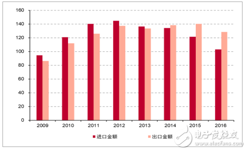
China PCB import and export situation
PCB production value transferred to the mainland

The PCB production capacity in Europe, America and Taiwan continues to shift to the mainland. The main reasons are as follows:
1. Western countries have tightened their environmental protection policies, and the relatively high-emission PCB industry has been forced to shift. Printed circuit boards contain heavy metal contaminants, which inevitably cause local environmental pollution during the manufacturing process. In Europe and the United States, the government's environmental requirements for PCB manufacturers are higher than domestic. Under strict environmental standards, enterprises need to establish a more complete environmental protection system, which will lead to an increase in corporate environmental protection expenditures, which will increase management costs and thus affect corporate profit levels. Therefore, European and American manufacturers only retain high-tech and confidential PCB business such as military and aerospace, as well as small-volume fast-board business, and continuously reduce the high-pollution, low-margin PCB business. The capacity of this part of the business has shifted to Asia, where environmental protection requirements are relatively loose and environmental protection expenditures are relatively low. Strict environmental policies have also hindered the release of new capacity. PCB manufacturers typically expand their production capacity by expanding their existing plants or new plants. On the one hand, the restrictions on environmental protection clauses have made it more difficult to locate a plant;
On the other hand, the increase in cost has reduced the expected rate of return of the project, weakened the feasibility of the project and increased the difficulty of fundraising. The speed at which European and American manufacturers invest in new projects is limited by the above two reasons and is lower than that of Asian manufacturers, which in turn releases relatively little new capacity and continues to lag behind the Asian region in PCB production capacity.
2. The mainland market gains price advantage with relatively low labor costs, and Western manufacturers tend to be inferior in price wars. The labor cost in the mainland market has a relatively low advantage. Although it has gradually increased in recent years, it is still far below the level of developed countries in Europe and America, and is also lower than the level of Japan and South Korea. With their own advantages in environmental protection and labor costs, mainland manufacturers can gain competitive advantage at a lower price than manufacturers in other regions, thereby expanding market share.
3. China has become the world's largest consumer electronics market, and the upstream and downstream industry chains are fully equipped with PCB industry demand. In the past ten years, China's electronic information industry has developed rapidly and the scale of the industry has continued to expand. In 2015, China's annual consumer electronics information manufacturing industry achieved a main business income of 11.1 trillion yuan, ranking first in the world. PCB is one of the carriers closest to the end product, and the demand in the mainland will continue to grow with the popularity of downstream end products. Correspondingly, the supply end of the mainland has also formed a complete industrial chain of “from copper foil, glass fiber, resin, to copper clad laminate, and finally to PCBâ€, which can support the growing production demand. Therefore, driven by demand, the industry's production capacity has been smoothly transferred to the mainland.
At present, China has formed a PCB industry gathering belt with the Pearl River Delta region and the Yangtze River Delta region as the core region. According to CPCA statistics, in 2013, there were about 1,500 domestic PCB industry enterprises, mainly distributed in the Pearl River Delta, Yangtze River Delta and Bohai Rim regions. The PCB production value in the Yangtze River Delta and Pearl River Delta regions accounted for about 90% of the total output value of mainland China. PCB capacity in the central and western regions has also expanded rapidly in recent years. In recent years, due to the increase in labor costs, some PCB companies have moved their production capacity from the Pearl River Delta region and the Yangtze River Delta region to the central and western cities with better basic conditions, such as Hubei Huangshi, Anhui Guangde, Sichuan Suining and other places. The Pearl River Delta region and the Yangtze River Delta region use their talents, economy, and industrial chain advantages to continuously develop into high-end products and high value-added products.
China PCB industry regional distribution

PCBs are multi-domain downstream and are less affected by a single application. For a long time to come, PCBs are still irreplaceable in electronic products. In general, PCBs in the global field are mainly used in large scale in the fields of computer, communication and consumer electronics. The market size of the three markets accounts for 70% of the total PCB application scale, and extends to the automotive, military and other fields. Data centers are moving toward high-speed, high-capacity, cloud computing, and high-performance features. The surge in data volumes such as IP, mobile broadband, network video, and cloud services has increased data traffic in data centers and has also driven data centers. Construction needs. According to IDC statistics, the global data center market reached US$45.2 billion in 2016, with a growth rate of 17%. The growth of China's data center is obviously faster than the global pace. In 2016, the scale was 71.45 billion yuan, with a growth rate of 37%, and the proportion increased from 8.6% in 2010 to 24.3% in 2016.
Production value forecast for various areas downstream of PCB (US$ million)

China's data center market size (100 million yuan)
Global data center market size (100 million US dollars)

Among the various PCB products required for high-end servers, HDI boards are relatively demanding. The HDI technology mainly requires the size of the printed circuit board, the width and width of the wiring, and the number of layers. It is the key to achieving high density of the PCB. At present, the share of HDI board in the domestic market is gradually rising, but there is still a huge gap with the production capacity of traditional multi-layer boards. As the user demands the data center to carry traffic and transmission speed, the demand of the server will increase the overall demand level of HDI.
HDI card in high-end server
The use of PCB in the server
China PCB market product structure changes
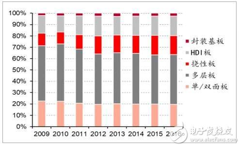
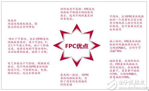
In the era of mobile Internet, smartphones, tablets and wearable devices are developing toward lightweight, miniaturized, multi-module, and wearable features. Based on the density advantages of HDI cabling over ordinary multi-layer boards, the demand for HDI boards for these products The amount will increase. The thin and light requirements of mobile electronic products have led to a reduction in the space of the motherboard, and it is possible to carry more components on the motherboard with limited requirements. Compared with the traditional multi-layer board, HDI adopts the laminated method to make the number of through-holes by blind holes and buried holes, saves the PCB's routable area, and greatly increases the density of components, thus quickly replacing it in smart phones. The original multi-layer board. The popularity of mobile electronic products such as smartphones will also drive demand for FPC boards. FPC is a flexible printed circuit board, which is a highly reliable and excellent flexible printed circuit board made of flexible copper clad laminate. It is a substrate for connecting electronic components and is also an electronic product signal. The medium of transmission. Under the trend of intelligent, light and thin mobile electronic products, FPC's high density, light weight, thin thickness, bending resistance, flexible structure and high temperature resistance will help it to be widely used.
Advantages of FPC
FPC has obvious advantages in the display module, touch module, fingerprint recognition module, side button and power button of the smart phone. About 14-16 FPCs are used in the new Apple phone, which together with other PCB materials account for $15 of the cost. Domestic mobile phone manufacturers such as Huawei, OPPO, and vivo have also increased the use of FPC in high-end flagship machines. The current usage is about 10-12 pieces, and future usage is expected to continue to increase under the trend of high-end.
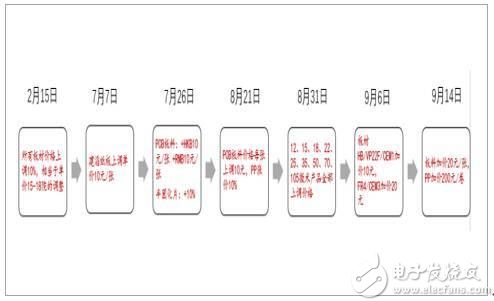
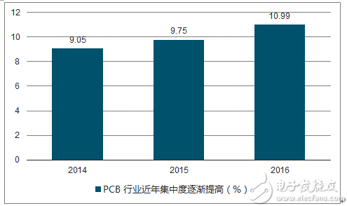
Under the “raw material price increase + environmental protection inspectorâ€, the concentration has increased, and leading manufacturers have welcomed the rising prices of raw materials to promote PCB prices.
Application scenario of FPC in iPhone
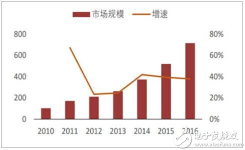
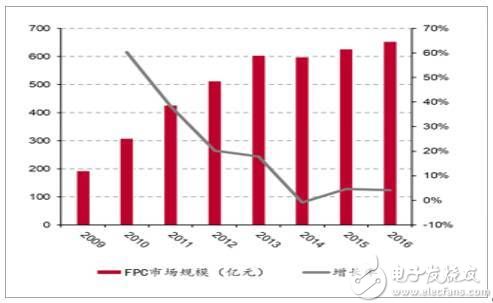
China FPC industry market size
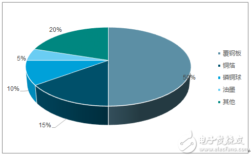
Raw materials in the PCB industry mainly include glass fiber yarn, copper foil, copper clad laminate, epoxy resin, ink, wood pulp, etc., in which the copper clad laminate is made of copper foil, epoxy resin, glass fiber yarn and other raw materials. Raw material costs in PCB operating costs account for a relatively large proportion, close to 60%. From the top to the bottom of the PCB industry chain is "raw material - substrate - PCB application", upstream materials include copper foil, resin, fiberglass cloth, wood pulp, ink, copper balls, etc., of which copper foil, resin and fiberglass cloth It is the three main raw materials; the midstream substrate mainly refers to copper clad laminates, which can be divided into rigid copper clad laminates and flexible copper clad laminates. The rigid copper clad laminates can be further divided into paper-based copper clad laminates, composite clad copper clad laminates and glass based on reinforcing materials. Fiber cloth-based copper clad laminates; downstream is the application of various types of PCBs, and the concentration of the industry chain from top to bottom is decreasing in turn.
Middle and lower reaches of the PCB industry chain

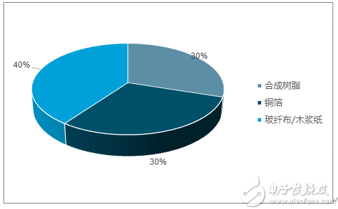
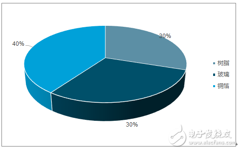
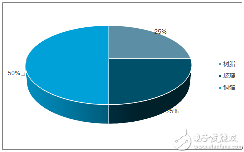
Industry upstream: Copper foil is the most important raw material for the production of copper clad laminates, accounting for about 30% (thick plates) and 50% (thin plates) of CCL costs. The price of copper foil depends on the price change of copper and is greatly affected by the international copper price. The copper foil is a kind of cathode electrolytic material, which is deposited on the base layer of the circuit board, and functions as a conductor of the PCB to conduct electricity and dissipate heat in the PCB. Glass fiber cloth is also one of the raw materials for copper clad laminates. It is made of fiberglass yarn and accounts for about 40% (thick plate) and 25% (thin plate) of CCL. Glass fiber cloth is used as a reinforcing material in PCB manufacturing to increase strength and insulation. In various types of fiberglass cloth, synthetic resin is mainly used as an adhesive to bond glass fiber cloth together in PCB manufacturing.
Thick copper clad material cost composition
Thin copper clad material cost composition

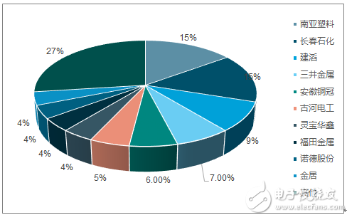
The copper foil production industry has a high degree of concentration and the industry has a strong bargaining power. The copper foil used in PCB production is mainly made by electrolysis. The process of electrolytic copper foil is long, the processing requirements are strict, there are capital and technical barriers, and after several integrations, the industry concentration is high, and the top ten production of global copper foil The occupies account for 73% of the output, and the bargaining power of the entire copper foil industry is strong. The price increase of the upstream raw material copper can be shifted downward.
Production share of the world's top ten electrolytic copper foil producers
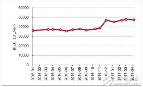
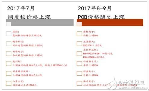
The first step of price increase is to transfer the raw material price to the lithium battery, and the price of copper foil continues to rise. Under the trend of rising copper prices, the supply of copper foil continued to be tight, and the price of copper foil continued to rise from last year (regardless of the stage of destocking of the 17Q2 industrial chain). At the same time, due to factors such as environmental supervision and rising cost of waste paper, the price of wood pulp paper is also rising.
The other raw material fiberglass manufacturers, driven by the demand of wind power, thermoplastics and other industries, rely on the bargaining power brought by the concentration of suppliers' capacity to raise prices. Recently, the shortage of glass cloth supply has further increased its price. The price of epoxy resin relative to the above raw materials is relatively stable. In 2016, due to the national new energy strategy, the demand for lithium batteries increased greatly. The key raw material electrolytic copper foil producers in PCB production transferred more than 15% of the production capacity to lithium batteries, resulting in PCB upstream CCL since the second half of 2016. Raw materials such as copper foil continue to rise in price.
Spot price trend of electrolytic copper since 2016
Thick copper clad laminate cost
Thin copper clad laminate cost
Copper price is rising in half a year

Wood pulp paper price index is on the rise
Midstream industry: CCL is the core substrate for PCB manufacturing. CCL is a kind of plate-shaped material which is made by impregnating the reinforcing material with organic resin and coated with copper foil on one or both sides. It is responsible for the three functions of (PCB) conduction, insulation and support. Special laminates made of PCB, CCL account for 20% to 40% of the total PCB production cost, accounting for the highest proportion of material costs of all PCBs. Fiberglass cloth substrates are the most common type of CCL, enhanced by fiberglass cloth. Material, epoxy resin is made of adhesive.
Cladding diagram

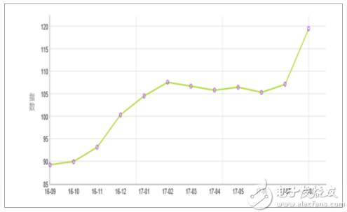
The second step of price increase: Due to the high concentration of CCL industry, the pricing power is basically in the hands of leading enterprises. Therefore, in the case of rising raw materials prices, CCL companies can conduct price transmission in time and transfer cost pressure to PCB manufacturers. . In light of the price changes of the above raw materials, CCL has started to rise in price from August 2016. Except for a slight price cut in March-June 2017, prices have continued to rise during the rest of the year. From the trend of price increases of major CCL manufacturers last year, the price hike will continue. The CCL faucet Jianye laminate was raised again on September 6, 2017. The price increase of FR4 CCL is as high as 20 yuan per piece. Other companies in the industry are also expected to follow the price increase.
CCL has been built frequently since 2017
At the same time, the price of liquid photosensitive solder resist ink, liquid photosensitive line ink price, thinner and other products used in the process of manufacturing PCBs also frequently rises. In the environment where the cost of various raw materials in the industry chain rises, the PCB cost is long-term. Will continue to rise. Downstream of the industry: The growth rate of traditional applications is slowing down, and emerging applications will become new growth points. The growth rate of traditional applications in the downstream of PCB is slowing down. In the emerging applications, with the increasing degree of electronic electronics, the large-scale construction of 4G and the future development of 5G, the construction of communication base station equipment, automotive PCB and communication PCB will become the new future. growth point.
4-layer PCB material cost composition
The third step of price increase conduction: PCB manufacturers can effectively transfer the price increase pressure to the terminal, complete the closed loop and ensure their own gross profit level. Leading companies continue to optimize management processes, improve operational capabilities, and accumulate advantages in many ways to respond to environmental changes. The advantages accumulated in the procurement, production and management organization capabilities help to reduce production costs and increase efficiency.
PCB price rises after copper price increase
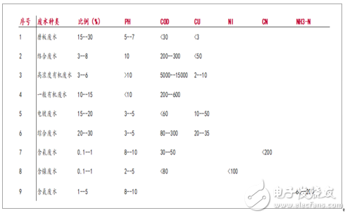
Certain waste water, waste gas and solid waste will be produced during the production of printed circuit boards. In order to control the increasingly serious pollution problem, China has made relevant regulations on the allowable emissions and emission concentrations of waste gas, waste water and waste residue (referred to as “three wastesâ€) discharged from industrial pollution sources, among which the problem of three wastes in the production process of printed electronic boards is proposed. Specific standard requirements.
PCB wastewater discharge standard
In July 2015, the 14th meeting of the Central Deep Reform Group reviewed and approved the “Environmental Protection Inspector Program (Trial)†and clearly established an environmental inspection mechanism. In the two years, through four batches of environmental inspectors, the environmental storm has covered 31 provinces without dead ends, a total fine of 1.27 billion yuan, 1489 people were detained, 17,174 people were interviewed, and 16,878 people were accountable. In order to reduce costs, PCB manufacturers lack scientific and reasonable pollution control methods and become one of the key targets of environmental protection inspectors. In order to cope with high environmental protection standards and strict environmental protection inspections, the leading faucet has established a special environmental protection department, formulated relevant environmental protection systems, and continuously increased and reformed the company's environmental protection projects and environmental protection equipment, and adopted effective treatment for various pollutants. Measures to win long-term policy dividends on a small scale.
The global printed circuit board industry is highly fragmented and has many manufacturers, but there is no market leader. The top 10 PCB manufacturers in the world have a market share of less than 35%, and the number one company has a market share of less than 6%. According to the statistics of China Printed Circuit Industry Association in 2016, there are about 1,500 PCB manufacturers in mainland China, among which the top ten companies have little difference in revenue capacity, which is characterized by a small overall volume. Only 137 PCB companies in the 1,500 companies have revenues of over 100 million. Most of them are small-scale producers with low revenues. The PCB industry presents a highly dispersed competitive landscape.
On the whole, the mainland PCB industry is also in a relatively dispersed state of competition, with a large number of third-tier manufacturers relying on price and a small number of small and medium-sized customers. Under the background of rising raw material prices and stricter environmental protection inspectors, the reshuffle of the PCB industry has brought about a concentration increase. Small manufacturers have weak bargaining power at the downstream, and it is difficult to digest upstream price increases. Business operations will become more difficult, and even raw materials will not be available. Small and medium-sized PCB companies will withdraw because of the narrowing of profit margins. In this round of PCB industry shuffling process, leading companies have the advantages of technology and capital, and are expected to expand their scale by expanding production capacity, mergers and acquisitions, and product upgrades. With its efficient production process, excellent cost control and direct benefit to the industry's concentration. The industry is expected to return to rationality and the industry chain will continue to develop healthily. In addition, leading companies benefit from technological innovation and also have an advantage in tax rates. A high-tech enterprise that has been qualified (reviewed) is eligible to apply for corporate income tax benefits and high-tech corporate income tax exemption and taxation preferential policies starting from the year when the validity period of the approval (review) is approved. The applicable tax rate is 15%. The tax incentive amount of the leading enterprises in the industry averages tens of millions of yuan per year, accounting for a significant proportion of the current profit.
Concentration increase in the mainland PCB industry
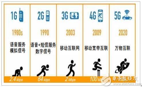
5G is the fifth-generation communication technology and is an extension of the fourth-generation communication technology (4G). The technical indicators of 5G are greatly improved compared with 4G. 1G was born in the 1980s, only supports voice calls, 2G implements SMS service, 3G makes mobile Internet a reality with its high transmission speed, 4G is produced in 2009, and 4G will reach 100Mbps in high-speed mobility environment. In the low-speed mobile environment, it is required to reach a rate of 1 Gbps to realize mobile broadband interconnection. On the basis of 4G, 5G will greatly improve various technical indicators. Among them, the peak transmission speed reaches 20Gbps, the delay is reduced to 1ms, the connection density reaches 106/km2, the mobility reaches 500km/h, and the traffic density reaches 10Mbps/m2.
Evolution of communication technology
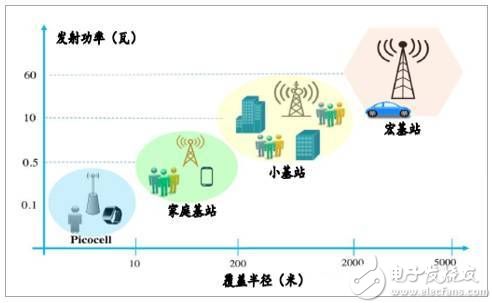
In the face of different requirements of 5G application scenarios, such as connection speed, delay, connection density, coverage and power consumption, 5G needs to be deployed in multiple frequency bands, so it needs to use a millimeter wave band with a wider spectrum and wider bandwidth (30GHz). The above) communicates. In order to solve the problem of short transmission distance of millimeter wave, the traditional macro base station deployment mode will change to a multi-layer ultra-dense networking mode combining macro base station-small base station-home base station, and large-scale antenna technology (Massive MIMO) passes a large Increase the number of antennas at the base station and the terminal to improve spectrum efficiency and reduce delay.
5G brings base station construction from macro base station to small base station
Due to the high operating frequency of millimeter waves, 5G new communication base stations have a large demand for high frequency circuit boards. High-frequency circuits usually refer to circuits with an operating frequency above 1 GHz. The characteristics of high-frequency boards must meet two requirements:
1. The dielectric constant must be small and stable, usually as small as possible, and a high dielectric constant tends to cause signal transmission delay.
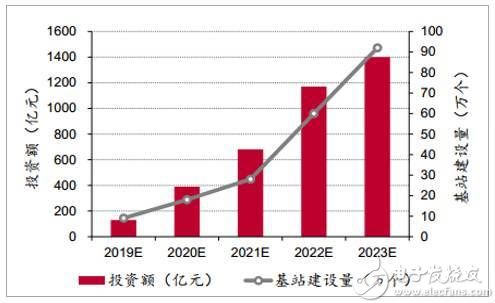
2. The dielectric loss must be small, which mainly affects the quality of signal transmission. The smaller the dielectric loss, the smaller the signal loss. These two points have very high requirements for the manufacturing process of high-frequency PCBs, so the technical barriers of high-frequency PCBs are higher, and the profit margin is much higher than other traditional PCB products. Millimeter wave development promotes the construction of thousands of small base stations. The 5G network transmission rate can reach 20Gbps, which is 200 times of the 4G peak. The higher transmission speed requires higher frequency band, but the higher frequency band has smaller electromagnetic wave coverage and weaker signal penetration, which means operators. To deploy more base stations, the base station scale in the 5G era is expected to exceed 10 million levels compared to the number of million-level base stations in the 4G era. The continued investment of communication operators in the next few years will bring about continuous growth in market demand.
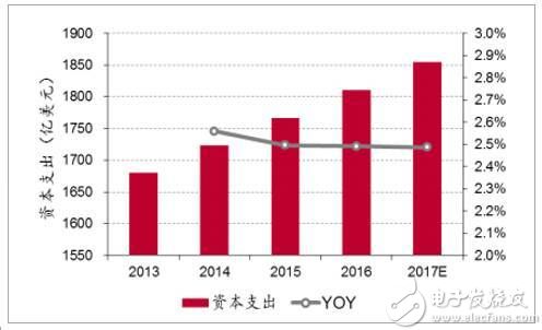
Global wireless communication capital expenditures in the past five years
Base station upgrades, 5G brings growth space for enterprise communication boards. With the advent of 5G commercialization, the mass construction and upgrading of communication base stations will have a huge demand for enterprise communication boards, and there will be massive upgrade and replacement requirements for PCBs.
Forecast of 5G base station construction from 2019 to 2023
Due to the complex working environment of automobiles, the reliability of automotive PCBs is extremely high. Secondly, there is a recall system in the automotive industry. Manufacturers need to bear the risk of product errors. Small-scale manufacturers cannot afford them, so they will be excluded. Moreover, the entry barrier of the vehicle PCB is high, and it must pass a series of verification tests, and the certification period is long. Once the certification is passed, the manufacturer generally does not easily change the supplier, and the order is relatively stable.
Top 10 automotive PCB companies in the world (ranking company's national/regional automotive PCB revenues (US$ million))
1. Jingpeng Industrial China Taiwan 545
2, TTMtechnologies United States 430
3, CMK Japan 390
4, MeikoElectronics Japan 380
5, Jianye Chemical Hong Kong, China 300
6, NipponMektron Japan 290
7, KCEElectronics Thailand 265
8, Jianding Technology China Taiwan 225
9, AT&S China Hong Kong 191
10. Hudian shares in mainland China 158
The trend of automotive electronics is driving the rapid growth of automotive PCBs. With the continuous advancement of the automobile industry, the automobile has evolved from a complete mechanical device in the past to a combination of machinery and electronics. The use of electronic technology in automobiles has increased, making the comfort, safety and entertainment of automobiles more important. Meet the diverse needs of people. The automobile has changed from a simple vehicle in the past to a comprehensive platform with various functions such as transportation, entertainment and office. The proportion of automobile electronics in the manufacturing cost of the vehicle is continuously increasing, and the market scale of the automobile electronics is also expanding. .
China's automotive electronics market scale and forecast
Automotive PCB market size and forecast
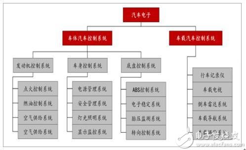
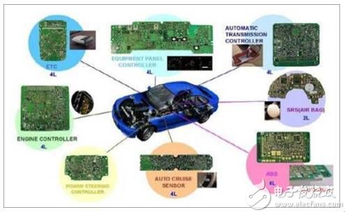
Automotive electronics can be divided into two main categories: vehicle body electronic control systems and vehicle electronic control systems. The vehicle body control system can be further divided into an engine control system, a vehicle body control system and a chassis control system. The vehicle body control system combines the automobile mechanical system with the electronic device, fully exploiting the advantages of the electronic product, improving the performance of the mechanical system, and ensuring the mechanical and electrical protection. The car is safer and more stable. The vehicle electronic control system mainly includes multimedia system, navigation system, driving recorder, parking sensor and other systems, which increases the convenience and entertainment of the car and enhances the experience of the car.
Classification of automotive electronic systems
The growth of automotive electronics will continue to drive automotive PCB demand. The electronic use of automobiles will increase the amount of PCB used in vehicles. At present, the PCB area of ​​the mid-range models is about 0.5-0.7 square meters, the economical automotive PCB area is 0.3-0.4 square meters, and the average bicycle value is about 60 dollars. The area of ​​automotive PCBs is about 2.5-3 square meters, and the value of bicycles exceeds 120 dollars. As the degree of electronic electronics deepens, the demand for automotive PCBs will gradually increase.
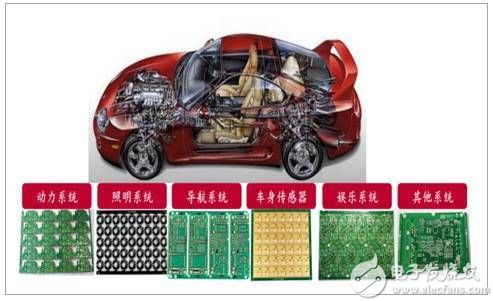
PCB application in the car
Intelligent driving has opened up more imagination for the automobile economy, and the penetration rate in the automotive market is increasing. The market for ADAS systems (Advanced Driver Assistance Systems) is growing rapidly, gradually merging into the mid-market from the original high-end market, and new and improved sensor technologies are creating new opportunities for system deployment. At present, the penetration rate of ADAS is less than 5%. With the further expansion of functions and the encouragement and even mandatory requirements of the policy, it is expected to grow at a rate of more than 20% in the future. By 2020, the market size is expected to approach 30 billion US dollars. A variety of operational control, safety control, and peripheral control functions in ADAS require PCBs. It is expected that fully automated vehicles will be equipped with more PCBs to meet driving needs in the future.
Application of PCB in ADAS system
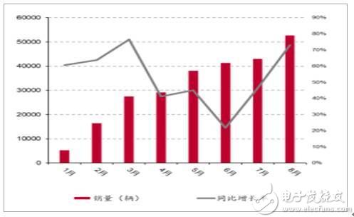
2017 new energy passenger car sales
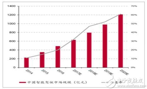
China's smart driving market size and forecast
The demand for PCBs for new energy vehicles is equally huge. With the support of industrial policies, the domestic new energy vehicle market has maintained rapid growth since 2014. Although the production and sales volume has been less than expected due to fraudulent compensation in 2016, the results of fraudulent investigations and the release of penalties and the adjustment of subsidy policies have been determined. Its production and sales are expected to resume rapid growth. BMS in new energy vehicles is one of the core components, and as one of the basic components of BMS, PCB boards will also benefit from the development of new energy vehicles.
China's new energy vehicle sales in the past five years
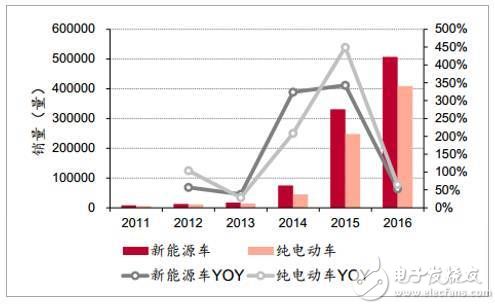
New energy vehicles are more electronic than traditional cars. New energy vehicles are represented by electric vehicles. Compared with traditional fuel vehicles, the main difference lies in the four major components, the drive motor, the speed controller, the power battery, and the car charger. The main purpose is to use the vehicle battery as the energy source and the motor as the power. The source drives the vehicle. Compared with traditional cars, new energy vehicles have higher requirements on the degree of electronicization. The cost of electronic devices in traditional high-class cars is about 25%, and in new energy vehicles, it is 45% to 65%.
The proportion of electronic equipment in the cost of the whole vehicle

New energy vehicle BMS: a new growth point for automotive PCBs. Lithium battery is the core energy source of new energy vehicles. In order to ensure the safe and reliable operation of the battery, the battery must be monitored in real time through the battery management system (BMS). BMS is also called the brain of electric vehicle battery system, with battery and body control. The system together constitutes the three core technologies of electric vehicles. PCB is the hardware foundation of BMS. The big bus has 12 to 24 boards, the small car has 8 to 12 boards, the main control circuit is about 0.24 square meters, and the single management unit is 2 to 3 square meters. Automotive PCBs will usher in volume as the market for new energy vehicles grows.
China's new energy vehicle BMS market size and forecast

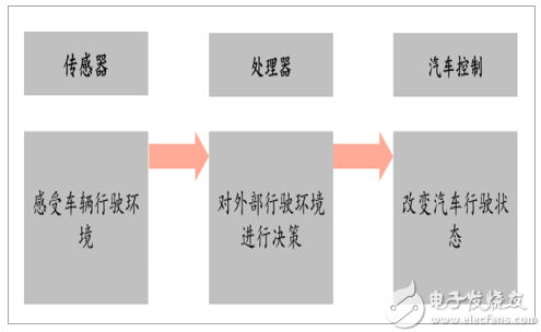
ADAS (Advanced Driver Assistance System) is a transition to the front of a fully self-driving car. It is a kind of sensor that is installed in the car and collects environmental data inside and outside the car at the first time. Technical processing such as identification, detection and tracking of dynamic objects, enabling drivers to detect possible hazards in the fastest time, to attract attention and improve safety, active safety technology, ADAS technical principle and human response The mechanism is similar. The surrounding information is obtained through the sensing layer, the information is processed by the decision-making link, and finally the calculation result is transmitted to the executing device to complete the driving operation.
Principle of ADAS reaction mechanism
The millimeter wave radar is the core sensor of the ADAS system. The millimeter wave radar refers to the radar working in the millimeter wave band. The radar is used to transmit radio to the surroundings, and the distance, direction and size of the obstacle are calculated by measuring and analyzing the reflected wave. Millimeter wave radar can be divided into 24GHz radar and 77GHz radar. The 77 GHz millimeter wave radar measures the speed of the vehicle ahead and the distance between the two vehicles. It also monitors the speed and distance of the vehicle. The 24 GHz millimeter wave radar is mainly used to monitor objects in the vicinity of the vehicle.
How does the car's millimeter wave radar work?

Millimeter wave radar throughput will bring huge demand for automotive high-frequency PCB. At present, the automobile millimeter wave radar is in a high-speed development. In the next two years, it will be in the heavy-duty period of the automobile millimeter wave radar. Generally, cars supporting the ADAS function will use at least 4 millimeter-wave radars, and the new Audi A4 will use 5 millimeter-wave radars. Mercedes-Benz S The grade car uses 7 millimeter-wave radars. It is expected that the average number of millimeter-wave radars in the future will continue to increase, and the demand for automotive radar PCBs will also grow rapidly.
Global automotive radar shipments

Millimeter-wave radar products are about to enter the heavy-duty period, requiring high-frequency PCB boards to implement the antenna's function—keeping the antenna with sufficient signal strength in a small integrated space. The higher specification of the high-frequency PCB board of the 77Ghz radar will bring about a huge demand for the corresponding high-frequency PCB board.
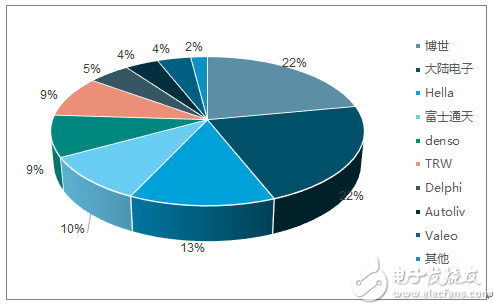
Market share of major manufacturers of global millimeter wave radar
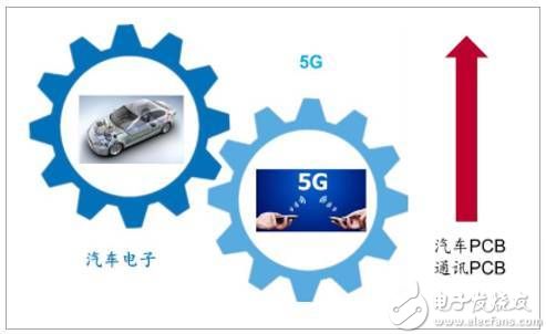
Car +5G promotes PCB growth
Busbar Type Switching Current Transformer
Busbar Type Switching Current Transformer,Clamp Type Current Transformer,Low Voltage Current Transformer,Low Voltage Switching Current Transformer
Zibo Tongyue Electronics Co., Ltd , https://www.tongyueelectron.com