In this issue, the author wants to talk about a familiar and somewhat strange content for analog engineers from the perspective of analog circuits: ESD Electrostatic discharge, also known as "static protection."
Wikipedia is defined as: Electrostatic discharge (ESD) is the sudden flow of electricity between two electrically charged objects caused by contact. Translated, it refers to the instantaneous current generated when two objects with stored charges contact each other.
Recently, the author's project, the requirements for ESD is more stringent, and often discuss with a buddy in the ESD department. He told me that ESD can happen anywhere, whether it is manufacturing, production, assembly, testing, or even transportation and field applications. At the time, I had an idea to give up treatment. . . .
So, the question is, how do we simulate and simulate it in the circuit? Generally, we are familiar with and need to use two models in circuit simulation: CDM and HBM.
CDM is the so-called Charge Device Model, and HBM is the so-called Human Body Model.
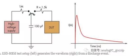
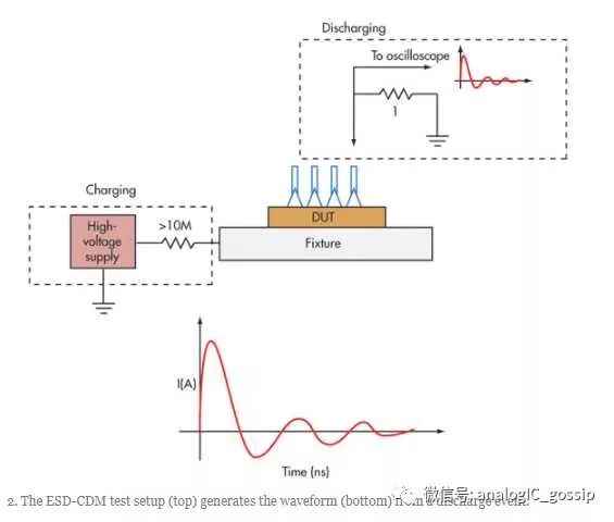
The comparison between the two shows that the current of the CDM is generally larger and faster than the current of the HBM because there is no large resistance to limit the discharge process on the discharge path.
Therefore, in the simulation of ESD, it is necessary to add such a pulse voltage to supply. For example, in a process situation: in the case of CDM, the supply needs to add a pulse of up to 15V, and the rising and falling edges are both 200ps for 4ns. In the case of HBM, the peak voltage of this pulse is only 6V, the rising and falling edges are 2ns, and the duration is 400ns.
Insert a sentence from the buddy here: "We are calculating the relevant value of this secondary ESD for you." After all, it was a matter of squatting, deep hiding and name. . . (To tell you nothing, don’t tell you how to count, mad at you...)
Wait, why did you come up with secondary ESD protection? Since there is secondary ESD protection, where is the primary ESD protection?
We are familiar with the IO structure, the kind of pad with a diode above and below, is the primary esd protection:
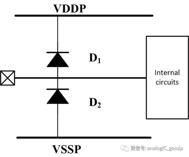
Universal IO with ESD protection
For example, in the HBM model, IO is added with a high voltage of +2000V, then the above diode D1 is naturally turned on, and the external high voltage is quickly guided away along the VDDP. Similarly, if a high voltage of -2000V is applied, D2 is turned on, and a large current flows from VSSP to IO quickly, and does not damage the internal circuit.
Here, the author wants to ask everyone a question: VDDP and VSSP are biased supply solutions for IO diodes. So what is the IO of VDDP and VSSP? Can you put a diode on top of each other?
Think fast after a second...
Certainly not like this! I feel that I can't do this...
There is no upper and lower two diodes, how to protect the IO of VDDP and VSSP?
Hey, let's take a look at the IO circuits of VDDP and VSSP!
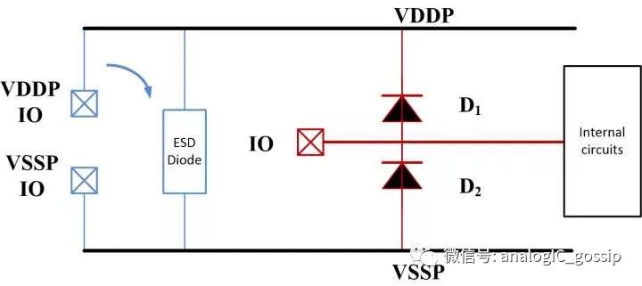
Including the IO ESD protection pad model
Therefore, there should be additional ESD protection circuits between IO of VDDP and IO of VSSP. For example, when VDDP is applied with a high voltage of +2000V, the high-voltage current is quickly guided through the ESD diode. And when VDDP is 0, and VSSP is added with a high voltage of +2000V, this...
Wait, let's think about it first. Is there two diodes in opposite directions?
......
After a second.
If VSSP is added +2000V, then not all IOs are very lively?
Why do you say that?
Hey, all nwells are biased to 0V by VDDP, and because the VSSP becomes 2000V, then isn't all the parasitic diodes between nwell and sub turned on?
Wow! Think about it, it sounds like a happy scene!
Then, the author heard that there is a so-called "1 Ohm" principle, it is said that the on-resistance from IO to those esd diodes must be less than 1 Ohm, so as to avoid too much parasitic resistance, affecting the effect of rapid discharge. To avoid some "slipping fish" flowing into the internal circuit. So if you look closely at the IO's layout, you will find that the metal is really dense, "all the best."
Finally, let's talk a little more about the circuit (too lazy to draw, so take it for borrowing):
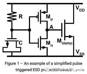
This is also an ESD protection circuit. Why do you want to say this? Because the author Jun was just asked to add a nmos switch on his internal circuit yesterday, the gate of the nmos is the point A in the figure. And it was told that this is also secondary ESD protection. (Please note that this fig.1 is part of io, the big nmos Mclamp is not an internal circuit. Here is the internal circuit that can be controlled using the internal nodes of io)
Let's briefly analyze: If there is a high voltage pulse on VDD, the voltage on the capacitor does not increase rapidly with VDD because of the voltage hysteresis of the capacitor. Therefore, the gate voltage of Mp is much smaller than the source at this time, causing Mp to be turned on, and point A is also connected to VDD. The large size of Mclamp is turned on, and VDD and VSS are connected by Mclamp. In this way, the pulse above VDD is thus led away by the huge Mclamp, so our fragile internal circuits are protected.
Go back to the place where the author was asked to add a switch. The nmos switch is similar to a power down function, but is controlled by point A in the figure. When there is a very serious ESD event, the internal circuit can be turned off quickly and shut down, and the high current of the ESD must not be available.
Finally, I recommend a doctoral thesis: http://ShuqingCao.pdftp://http://ShuqingCao.pdf
In this paper, it is also very detailed how the so-called ESD Design Window is getting smaller and smaller as the process shrinks. Because the size of the gate oxide is getting smaller and smaller, the breakdown voltage of the gate is also smaller, and the range in which the ESD protection can be used is getting smaller and smaller. It sounds very pitiful!
According to the author's comparison, the IO of 0.18um and the IO of 28nm are not very different (even 28nm seems to look bigger). It took so much effort to reduce the size of the process, even if the internal circuit became smaller, it was bottlenecked by the area of ​​the IO. This is a sad story!
Finally, one more sentence: ESD often needs tradeoff between it and leaveage. The esd diode is too large, the protection is better, and the leakage becomes worse, affecting the performance during normal operation. Weigh the pros and cons when you need to use it.
This 60 -port USB charger is charged at the fastest speed to as many as 60 devices. The table charger has 60 ports. The maximum output of a single USB port is 2.4A, and the output power is as high as 300W. Super intelligence: Each port can charging a current of up to 2.4A, and adaptive smart chip detector can provide the best charging current for connected devices. Multiple protection: The USB charger has rush protection, over -current and overvoltage protection functions, which can safely protect your smart devices. Suitable for multiple devices: charging stations are compatible with 99 % of smart devices, such as iPad iPhone, tablet, Bluetooth headset, fan, DVS, for PSP. It is suitable for various occasions, such as hotels, school dormitories, gym and other places.

60 Port Usb Charger,60 Port Portable Hub,60 Port Usb Smart Charger,High Power Mobile Phone Charger
shenzhen ns-idae technology co.,ltd , https://www.best-charger.com