Abstract : For 28nm and below nodes, the complex requirements of selecting and placing multiple via types pose challenges to the winding of LEF/technical documentation, resulting in increased design rule checking (DRC) errors (which take time to debug and correct) , ultimately affecting yield and performance.
For the 28nm and below nodes, various new design requirements have forced us to adjust the traditional digital board diagram design and verification process. In particular, the use of vias has been greatly affected. New via types have been introduced, and the addition of double patterning, FinFETS, and other new design techniques not only significantly increases the use of vias, but also leads to the selection and placement of via types used to define layouts. The number and complexity of design rules has increased. The layout and routing (P&R) issues in advanced node processes are becoming more and more challenging, and our current chip layout and verification methods are beginning to keep up with demand.
Via failure has always been a significant factor affecting yield. Via redundancy (double vias) is introduced into the 65nm layout design to help reduce via failures caused by variations in the manufacturing process. For the 28 nm node, we added a rectangular via (sometimes called a strip via). Replacing a single via with a rectangular via instead of a double via prevents stub failure and reduces the total number of vias. Figure 1 shows three via types.
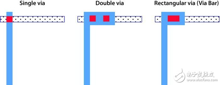
Figure 1: The number of via connections is increasing
Reducing the number of vias is important because the number of conventional vias required for node design at 28 nm and below is significantly increased. There are two main reasons for this: First, the number of metal layers at 28 nm and below is significantly increased, requiring more Second, these design nodes have new design requirements. For example, due to the necessity to decompose the geometry, the dual imaging layer may increase the number of vias required, and the electron mobility limitations require more different types of vias for the power/ground lines.
As the number of vias increases, the number and complexity of rules required to ensure proper placement and selection of vias during place-and-route is also significantly increased. There are four main reasons for the rapid increase in the complexity of via insertion:
In small node designs, wiring is more challenging, requiring not only new configurations (these configuration big node designs are less common), but also factors that were not important in previous big nodes. For example, at the 20 nm node, the choice of vias requires simultaneous evaluation of metal ends -1 and +1. Winding is no longer just to optimize the vias, but to consider both the upper and lower metal and the direction in which the vias connect the metal.
More via types increase the choice of vias that can be used for winding. More winding rules are needed to define when a particular via is used and how it is used.
The foundry defines via prioritization – each foundry has proprietary rules for selecting specific via types. Although the routing rules allow for selection between multiple via types, the foundry priority rules govern the order of these types based on geometry, environmental characteristics, via wrapping, and many other variables. In addition, these priorities may change rapidly in the development of process nodes, and the winding rules need to be constantly updated.
Double patterning – The double patterning requirement affects the placement and orientation of the vias and must be considered during the layout and routing stages.
But why are these problems? Does the winding tool have no winding rules to tell how and where to place layout elements?
In the digital world, detailed routing rules are often simplified approximations of design rules so that they can be encoded as a Library Exchange Format (LEF) specification or a technical file for a winding tool. Winding tools typically use these simplified DRC and DFM rules to achieve the best balance of run time and accuracy during the winding process. Once the winding is complete, the GDSII layout is verified using the signed-quality DRC/DFM rules file and the standard verification rule format (SVRF) rules platform. This can be sufficient for the previous node because the number of violations found during the sign-off confirmation is relatively low.
As the new process node matures, the factory design rules file for the SVRF language representation used by the sign-off engine is continually updated to address the manufacturing issues found. Ultimately, these factory sign-off models and platforms are essentially the most accurate and complete representation of actual manufacturing needs. The layout and routing tool usage rules expressed in LEF/technical documents are simpler and often do not synchronize with manufacturer rules. In addition, for the 28nm and below nodes, there are some rules that cannot be expressed in the simpler LEF/technical file language. Therefore, the routing tool will report that the layout does not violate the DRC/DFM rules, but the sign-off analysis found a large number of violations. Debugging and correcting after layout and routing is not only time consuming and resource intensive, but the changes that are being made to handle them can also lead to new manufacturing violations or negatively impact the design's target performance.
For nodes of 28 nm and below, the rules governing the selection and placement of vias are much more complex than the graphs (Figure 2). Not only are there more rules, but the rules are more complicated. As discussed, there are many types of vias to choose from, as the case may be. Each foundry has its own priorities, which determines which via type it will choose. In addition, via placement may also be affected by design factors such as dual imaging.
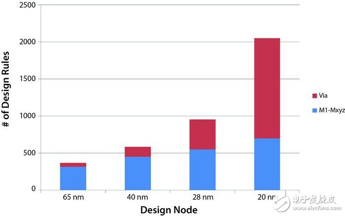
Figure 2 Winding tools are facing the challenge of increasing the number of via rules and increasing their complexity
The requirements for new processes related to via selection are not only very numerous, but they are quite complex to implement. If you are using a rectangular via, how do you place a via array? When dealing with double pattern requirements, how to accurately determine whether the via is wrapped? Not only do LEF/technical documents need to be able to understand and respond to these situations, but they must also be able to understand and adapt to specific plant requirements for priorities, selection order, via orientation and vias. For each pass of the routing tool, you must determine the layout options and then understand the plant's prioritization to determine the correct via selection and placement. In addition, as discussed earlier, these priorities may change frequently and require frequent updates to the routing rules.
So what will the designer do? Even if you make the most of the winding system tools, for example, using LEF/technical files to achieve about 80% of the via placement, you will still miss about 20% of what you need to do to optimize. Hole selection and layout. Of course, as you learned at school, such a 20% is usually the most difficult and challenging via optimization, with the greatest potential for yield impact. Even though these factory-certified utilities help you successfully eliminate and correct these via problems, how much time and effort does it take to accurately target the design layout file (DEF)?
However, there is still hope. Recent advances in technology have enabled these foundry-proven utilities to automatically address these complex via placement issues to comply with DRC/DFM rules, and to automatically reverse these changes to the original layout and routing DEF. It is feasible. In the near future, designers will be able to ensure 100% via optimization for the design efficiently, accurately, and quickly during the layout and routing phases of the design process.

Jean-Marie Brunet is Director of Product Design and Layout Integration Product Marketing at Mentor Graphics, Wilsonville, Oregon.
LED Street Light which semiconductor lighting, light emitting diode as light source, because it is a solid cold light source, green pollution-free, less consumption, high luminous efficiency, long service life etc, made of LED street light.
LED Street Light is applicable to road, highway, highways, urban streets, sidewalks and other road lighting and square, schools, industrial zone, parks and other outdoor lighting.
LED Street Light
LED Street Light,LED Solar Street Light,Adjustable LED Street Lighting,Solar Panel LED Street Light,Outdoor Light
Wenzhou Korlen Electric Appliances Co., Ltd. , https://www.korlenelectric.com