First, the integrated gate circuit
Digital integrated circuits can be divided into two categories according to their internal active devices: one is a bipolar transistor integrated circuit (TTL circuit); the other is a unipolar integrated circuit (a circuit composed of MOS transistors).
1. TTL integrated logic gate
(1) TTL NAND gate
The circuit composition of CT74S Schottky series TTL NAND gate is shown in Figure 2-19(a). It consists of three parts: input stage, intermediate stage and output stage.
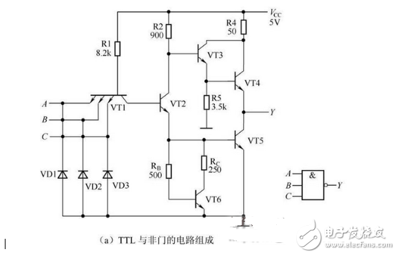
Figure 2-19 TTL NAND gate circuit diagram
Input stage: consists of multiple emitters VT1 and resistor R1. The three emitter junctions of the multiple emitters are three PN junctions. Its role is to achieve a logical AND of the input variables A, B, C, so it is equivalent to an AND gate.
Intermediate stage: consists of VT2, R2 and VT6, RB, RC. The VT2 collector and emitter simultaneously output two signals with opposite logic levels to drive VT3 and VT5.
Output stage: It consists of VT3, VT4, VT5 and R4, R5. It adopts Darlington structure. VT3 and VT4 form a composite tube to reduce the output resistance when outputting high level, which improves the load capacity.
The logical symbols of TTL NAND gates are shown in Figure 2-19(b); the logical expression is: 
For the circuit shown in Figure 2-19, if the high level is indicated by 1 and the low level is represented by 0, the truth table shown in Figure 2-19 can be listed, as shown in Table 2-1.
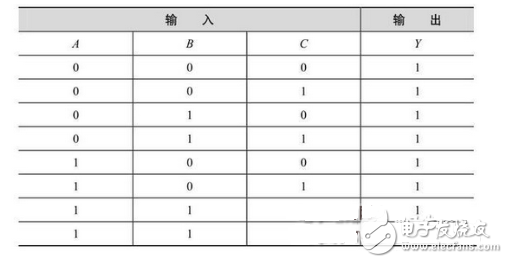
Table 2-1 TTL and NOT gate truth table
(2) Open collector NAND gate (OC gate)
1 Working principle.
The open collector NAND gate is also called the OC gate, which can make the output voltage of the gate circuit higher than the high voltage value of the circuit, and the output terminals of the gate circuit can be connected in parallel to realize the logic and function, that is, the line and (general TTL gate The circuit cannot be wired with).
The circuit of the OC gate is shown in Figure 2-20(a). The logical symbol is shown in Figure 2-20(b). The logical expression is:
Figure 2-20 Open collector NAND gate and logic symbol
2 OC door application.
The OC gate can implement line and, as shown in Figure 2-21, the logical expression is ![]() Drive the display to achieve level shifting, as shown in Figure 2-22.
Drive the display to achieve level shifting, as shown in Figure 2-22.
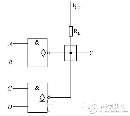
Figure 2-21 Using the OC gate to achieve line and
(3) and the right or wrong door
The NAND gate circuit is shown in Figure 2-23(a). The logic symbol is shown in Figure 2-23(b). The logical expression is:
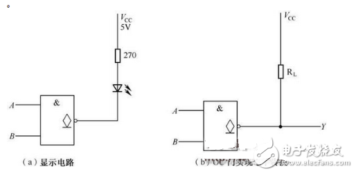
Figure 2-22 Driving the display to achieve level shifting
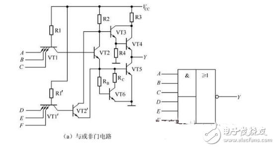
Figure 2-23 and NOR gates and logical symbols
(4) Three-state output gate
The three-state output gate refers to a gate circuit that can output not only the high level and the low level but also the high resistance state, as shown in Figure 2-24. ![]() For the console.
For the console.
when ![]() =0, G output P=1, VD cutoff, output Y=
=0, G output P=1, VD cutoff, output Y= ![]() The three-state door is in working condition.
The three-state door is in working condition. ![]() Active low.
Active low.
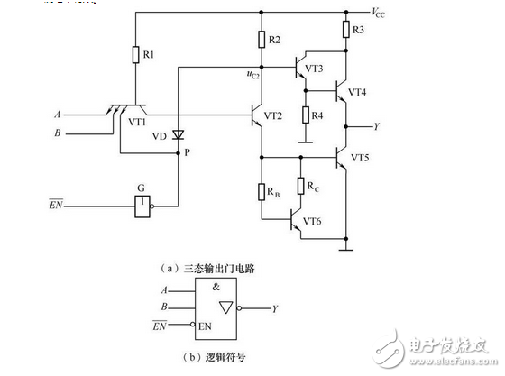
Figure 2-24 Three-state output NAND gate and its logical symbols
when ![]() When =1, G output P=0, VD is turned on, and the high-impedance state is output.
When =1, G output P=0, VD is turned on, and the high-impedance state is output.
2. CMOS integrated logic gate
Compared with TTL digital integrated circuits, CMOS circuits are characterized by micro power consumption and high anti-interference ability.
(1) CMOS inverter
The two FETs form a complementary working state, as shown in Figure 2-25. The logical expression is:
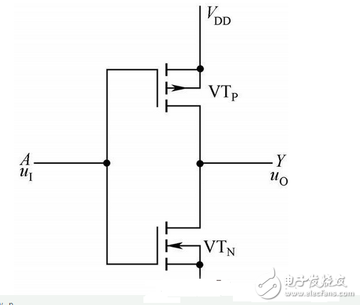
Figure 2-25 CMOS inverter
(2) CMOS NAND gate
As shown in Figure 2-26, two series-connected enhanced NMOS transistors VTN1 and VTN2 are drive tubes, and two parallel enhanced PMOS transistors VTP1 and VTP2 are load tubes to form a CMOS NAND gate. The logical expression is:  .
.
(3) CMOS or NOT gate
As shown in Figure 2-27, two parallel enhanced NMOS transistors VTN1 and VTN2 are drive tubes, and two series-connected enhanced PMOS transistors VTP1 and VTP2 are load tubes to form a CMOS NOR gate. The logical expression is:
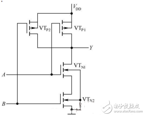
Figure 2-26 CMOS NAND gate
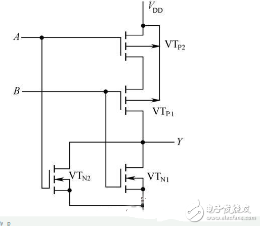
Figure 2-27 CMOS NOR gate
(4) CMOS transmission gate
A two-parameter symmetrical NMOS transistor VTN and a PMOS transistor VTP are connected in parallel to form a CMOS transmission gate. The circuit and logic symbols are shown in Figure 2-28.
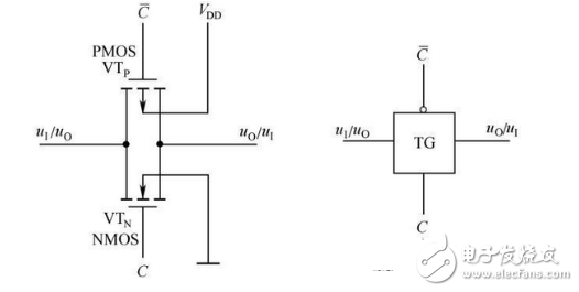
Figure 2-28 CMOS Transmit Gate and Logical Symbols
(5) CMOS tri-state gate
Figure 2-29(a) shows the low-level controlled tri-state gate output, and Figure 2-29(b) shows the logic symbol.
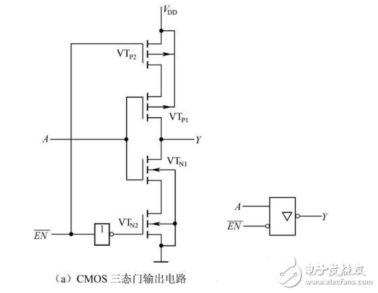
Figure 2-29 CMOS Tri-State Gate Output and Logic Symbols
when ![]() When VTP2 and VTN2 are turned on, CMOS inverters composed of VTN1 and VTP1 work, so
When VTP2 and VTN2 are turned on, CMOS inverters composed of VTN1 and VTP1 work, so  .
.
when ![]() VTP2 and VTN2 are turned off at the same time, and the output Y is high impedance to the ground and to the power supply VDD.
VTP2 and VTN2 are turned off at the same time, and the output Y is high impedance to the ground and to the power supply VDD.
(6) CMOS XOR gate
Figure 2-30(a) shows the XOR gate, and Figure 2-30(b) shows the logic symbol.
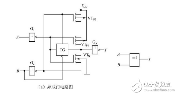
Figure 2-30 CMOS XOR gate and logic symbol
When the input A=B=0 or A=B=1, the input signal is the same, the output Y=0; when the input A=1 or B=1, the input signal is different, and the output Y=1. Its truth table is shown in Table 2-2.
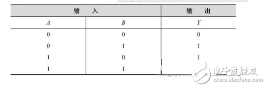
Table 2-2 XOR gate truth table
3. Composite gate
In addition to the logic gates described above, there are also NOR gates, XOR gates, and OR gates. Table 2-3 is the logical symbols, logical expressions, and logic functions of the basic gates and common composite gates.
Table 2-3 Comparison table between basic door and common composite door
Second, the combination of logic circuits
The output state of the logic circuit at any time depends only on the input state at this moment, and regardless of the original state of the circuit, the circuit is called a combinational logic circuit.
1. Analysis method of combinatorial logic circuit
(1) Analysis steps
1 Write out the output logic relationship according to the given logic circuit. Generally, the logical expression of each gate output to its input is written step by step from the input end to the output end, thereby writing the logical function formula of the output of the entire logic circuit to the input variable. If necessary, you can simplify and find the output logic function.
2 List the truth table for the logic function. The state of the input variable is substituted into the output logic function in a natural binary number order, and the corresponding output state is obtained, and the table is filled in, that is, the truth table is obtained.
3 Analyze the logic circuit based on the truth table and logical expressions, and finally determine its function.
(2) Analysis example
Analyze the function of the logic circuit shown in Figure 2-31.
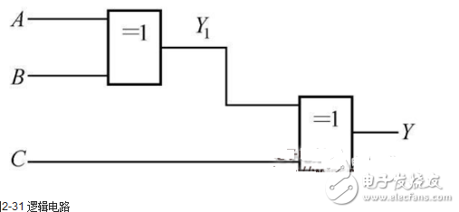
Figure 2-31 Logic circuit
1 Write the output logic function expression:
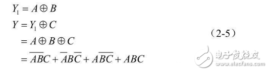
2 List the truth table for the logic function. The various combinations of the values ​​of the inputs A, B, and C are substituted into the equation (2-5), and the value of the output Y is obtained. The truth table is listed here, see Table 2-4.
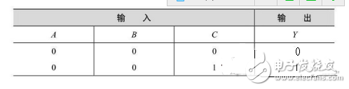
Table 2-4 Truth Table
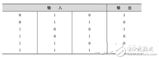
Continued
3 logical function analysis. It can be seen from Table 2-4 that when there are an odd number of 1 in the three variables A, B, and C, the output Y is 1, otherwise Y is 0. It can be seen that Figure 3-34 is the three odd schools. Check the circuit.
2. Design method of combinational logic circuit
(1) Design steps
The design of the combinational logic circuit should aim at the simple circuit and the minimum number of devices used. The design steps are as follows:
1 Analyze design requirements and list truth tables;
2 Write an output logic function expression according to the truth table;
3 Simplify the output logic function;
4 Draw a logic diagram based on the simplest output logic function.
(2) Design example
Design an A, B, C3 personal voting circuit. When voting on a proposal, the majority agreed that the proposal was passed and A had a veto. Realized with NAND gates.
1 Analyze the design requirements and list the truth tables, see Table 2-5. Let A, B, and C agree that the proposal is represented by 1, and disagree with 0, Y is the result of voting, and the proposal is 1 and not 0.
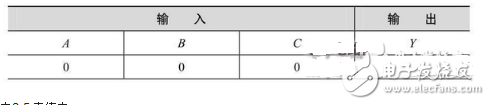
Table 2-5 Truth Table
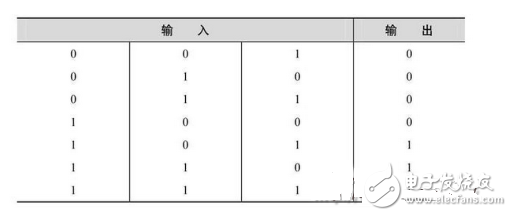
Continued
2 Simplify the output logic function and convert it to a non-expression. Simplified by the Karnaugh map in Figure 2-32.
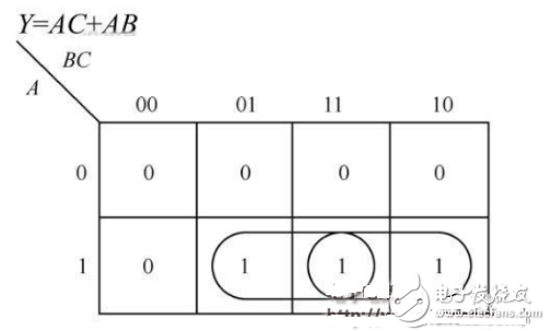
Figure 2-32 Karnaugh map
Change the above expression to a non-expression
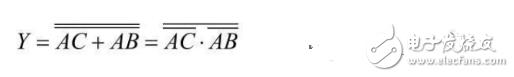
3 Draw a logic diagram according to the output logic function (2-6), as shown in Figure 2-33.
3. Competitive adventure in combinatorial logic
(1) Competitive risk phenomenon and its causes
When the signal passes through the wire and the gate circuit, there is a delay in time, and there is also a certain rise time and fall time when the signal changes. Therefore, a set of input signals of the same gate, through a different number of gates, through the transmission of wires of different lengths, the time to reach the input of the gate will be preceded, this phenomenon is called competition.
Figure 2-33 Logic circuit
The logic gate causes the output to produce an undue spike interference pulse (also known as a transient interference pulse) due to competition at the input, which is called adventure. As shown in Figure 2-34.
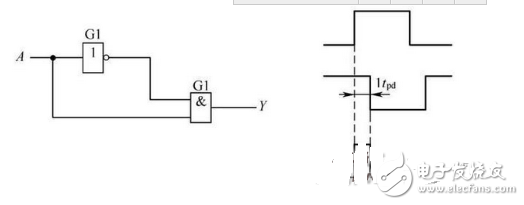
Figure 2-34 Generate a positive spike interference pulse adventure
(2) Discrimination of risk phenomena
In the combinational logic circuit, whether there is an adventurous phenomenon can be discriminated by a logic function. If the output logic function written according to the combinational logic circuit can be simplified into the following two forms under certain conditions, then the combinational logic circuit has an adventurous phenomenon, namely:
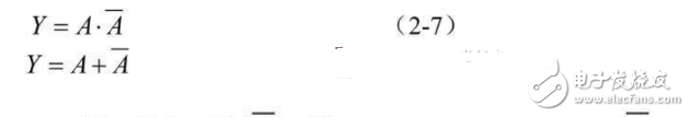
For example, functional  , when A=C=0,
  . If the logic circuit is directly composed according to this logical expression, a competitive risk may occur.
(3) Ways to eliminate the phenomenon of risk
1 Add extra items. E.g:  When A=1, C=1, there is a competitive risk. According to the basic formula of logical algebra, adding an AC, the functional formula is unchanged, but eliminates the competitive risk, that is,
 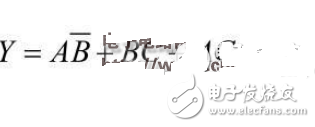 .
.
2 Add a blocking pulse. During the competitive time of the input signal generation, the introduction of a pulse locks the door that may produce a spike interference pulse. The blocking pulse should arrive before the input signal is converted and disappear after conversion.
3 Add a strobe pulse. An input terminal for inputting a strobe signal is input to a gate circuit that inputs a peak interference pulse. Only after the input signal conversion is completed and stabilized, a strobe pulse is introduced to turn it on, and an output is allowed at this time.
4 Connect the filter capacitor. If the logic operates at a slower speed, a capacitor can be connected in parallel with the output. Since the width of the spike interference pulse is generally narrow, the peak interference pulse can be absorbed by the capacitor.
5 Modify the logic design.
Third, the sequential logic circuit
Unlike combinatorial logic, the output state of a sequential logic at any one time depends not only on the input signal at the time, but also on the original state of the circuit.
1. Analysis method of synchronous sequential logic circuit
(1) Analysis steps
1 Write the equation. Write the output logic expression of the sequential logic circuit (ie, the output equation), the logic expression at the input of each flip-flop (ie, the drive equation), and the state equation of the sequential logic circuit.
2-column state transition truth table. The various values ​​of the current state of the circuit are substituted into the state equation and the output equation to calculate, and the corresponding secondary states and outputs are obtained, thereby listing the state transition truth table.
3 Description of the logic function. The logic function of the circuit is explained according to the state transition truth table.
4 Draw a state diagram and a timing diagram.
(2) Analysis example
Analyze the logic functions of the circuit shown in Figure 2-35 and plot the state transition diagram and timing diagram.
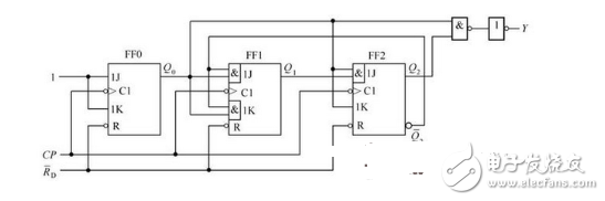
Figure 2-35 Diagram of the logic to be analyzed
1 Write the equation:
Output equation: ![]()
Drive equation: 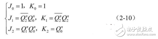
Equation of state: Substituting the driving equation into the characteristic equation of the JK flip-flop Qn+1= ![]() , get the state equation of the circuit as
, get the state equation of the circuit as
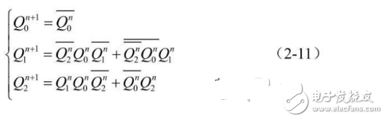
2-column state transition truth table: The current state of the circuit is ![]() Substituting into the output equation (2-9) and the equation of state (2-11) to obtain Y=0 and
Substituting into the output equation (2-9) and the equation of state (2-11) to obtain Y=0 and ![]() And then substitute 001 as the current state into the equation of state (2-11).
And then substitute 001 as the current state into the equation of state (2-11). ![]() And so on. The state transition truth table shown in Table 2-6 can be obtained.
And so on. The state transition truth table shown in Table 2-6 can be obtained.
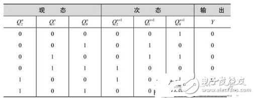
Table 2-6 Status Conversion Truth Table
3 Logic function description: As can be seen from Table 2-6, the circuit shown in Figure 2-35 is input to the sixth count pulse CP, returning to the original state, and the output terminal Y outputs a carry pulse. Therefore, the circuit is a synchronous hex counter.
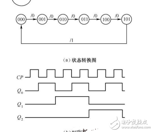
Figure 2-36 State transition diagram and timing diagram
4 Draw state transition diagrams and timing diagrams. The state transition diagram shown in Figure 2-36(a) can be drawn according to Table 2-6. The circle in the figure indicates a state of the circuit, the arrow indicates the state transition direction, the X/Y is marked as the transition condition above the arrow line, X is the value of the input variable before the conversion, and Y is the output value. Since there is no input variable in this example, X is not marked with a value.
2. Design method of synchronous sequential logic circuit
The design and analysis of synchronous sequential logic circuits is just the opposite, designing synchronous sequential logic circuits based on the requirements of a given logic function. The key to the design is to determine the law of state transitions and to determine the drive equations for each trigger based on design requirements.
Ethernet cables connect devices such as PCs, routers, and switches within a local area network.Most technicians refer to these standards as CAT5 and CAT6, respectively. Also CAT3 available. Because of this, many online stores that sell network cables use this abbreviated language as well.
The connector can by shield or non-shield type, raw cable can be UTP, STP, FTP type. Also the molded shape can be custom mould by straight, right-angle, 105 degree, etc.
These physical cables are limited by length and durability. If a network cable is too long or of poor quality, it won't carry a good network signal. These limits are one reason there are different types of Ethernet cables that are optimized to perform certain tasks in specific situations.
Ethernet Cable Wiring,RJ45 cable,networking cable,8P8C cable
ETOP WIREHARNESS LIMITED , https://www.wireharnessetop.com