In modern digital communication, the modulation technique uses a non-constant envelope modulation method, where the peak and average values ​​are significantly different and described as a peak-to-average ratio (PAR). In order to meet the linearity requirement, power backoff is often used. Increase linearity. With the power back, the efficiency of the amplifier's efficiency will also be greatly reduced. Applying Doherty technology to RF power amplifiers can significantly increase the efficiency of the system.
The traditional Doherty amplifier proposes to connect a carrier amplifier and a peak amplifier with a quarter-impedance conversion line to improve the efficiency of the power amplifier and the circuit structure is relatively complicated. At the same time, compensation lines need to be added after the peak amplifier and carrier amplifier link. When the small-signal stage, the compensation line behind the peak amplifier is used to transform the small impedance of the peak amplifier into a large impedance to achieve an open circuit state, so that the Doherty power amplifier is Both high power and low power state can well match the load impedance and achieve high efficiency. In this paper, a 3dB hybrid bridge is proposed to replace the 1/4 impedance transform line and compensation line in the traditional circuit, which makes the circuit simpler, simplifies the debugging process, and improves the production feasibility and system reliability.
2. Principle of Doherty Power AmplifierThe concept of the Doherty power amplifier was first proposed by William H. Doherty of Bell Labs. At first it was applied to a vacuum tube amplifier. The block diagram of the classic Doherty amplifier is shown in Figure 1. The circuit includes a 3dB splitter, two 1/4-wavelength microstrip lines, and a main amplifier and auxiliary amplifier. Among them, the 1/4 wavelength microstrip line before the auxiliary power amplifier achieves a phase lag of 90 degrees with respect to the input current of the main power amplifier, and the 1/4 wavelength microstrip line behind the main power amplifier is more important while compensating for the output phase difference. It plays a role in impedance transformation.
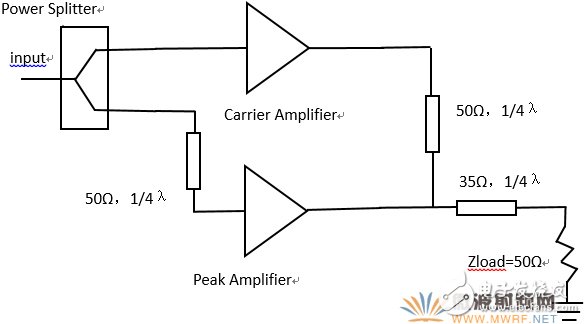
Figure 1, the basic block diagram of the Doherty amplifier
The carrier amplifier operates in Class B or Class AB, and the peak amplifier operates in Class C. When the input signal is relatively small, the peak amplifier is turned off and only the carrier amplifier is in operation; when the output voltage of the tube reaches the peak saturation point, theoretically Efficiency can reach π/4. If the excitation is doubled at this time, then the amplifier will saturate at half the peak value and the efficiency will reach the maximum π/4. At this time, the peak amplifier will start to work together with the carrier amplifier. The introduction of the peak amplifier, from the carrier amplifier point of view, the load is reduced, because the role of the peak amplifier on the load is equivalent to a negative resistance in series, so even though the output voltage of the carrier amplifier is saturated, the output power is reduced because of the load. Small but continuous increase (the current flowing through the load becomes larger). When the peak of the excitation is reached, the peak amplifier also reaches the maximum point of its own efficiency, so that the efficiency of the two amplifiers together is much higher than the efficiency of a single Class B amplifier. The maximum efficiency π/4 of a single Class B amplifier appears at the peak, and now the efficiency of π/4 appears at half the peak (6 dB back off). So this structure can achieve high efficiency (Figure 2).
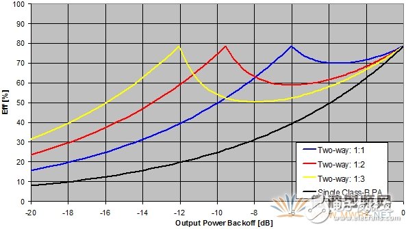
Figure 2. The highest efficiency point of different power ratios for carrier and peak amplifiers
In practical applications, the gain of the Doherty amplifier has a significant decrease in gain compared to a single tube at low power input. The main reason is: due to the influence of the peak amplifier matching circuit, when the peak amplifier is cut off, its equivalent impedance does not satisfy the infinite condition of the ideal situation. And because the equivalent impedance is not ideally infinite, the power of the carrier amplifier leaks and the efficiency is reduced.
In order to solve the Doherty amplifier in the case of small signal, the carrier amplifier does not meet the ideal condition of cutoff, usually the offset line is added to the input and output of the peak amplifier and carrier amplifier link, and the compensation line after the carrier amplifier is used for small When the signal is drained to achieve a large current, it can achieve the effect of early saturation and increase efficiency. The compensation line behind the peak amplifier is used to transform the small impedance of the peak amplifier into a large impedance to achieve an open circuit state. Therefore, it is extremely important whether the length of the compensation line is appropriate. In modern mobile communications, the frequency is always 2GHz, 3GHz, and its one wavelength is only several tens of millimeters. The difference of several millimeters in the compensation line will cause a great difference in performance. The length of the compensation line is also the debugging of the Doherty circuit. difficulty. The main role of the compensation line at the input is to allow the two amplifiers to maintain the same phase at the output combiner for efficient power synthesis.
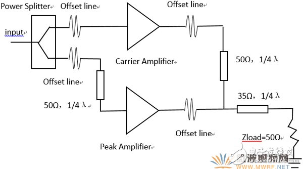
Figure 3. Practical application diagram of Doherty power amplifier
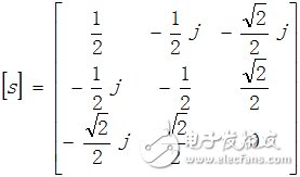
3, improved Doherty power amplifier principleAs can be seen from Figure 1, the output combiner of the traditional Doherty power amplifier circuit uses a bifurcated combiner. In the dashed box of the figure, the S-parameter matrix of this circuit is
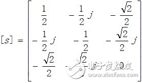
(1)
The output combiner of the Doherty amplifier can also be made using a 3dB hybrid bridge, as shown in Figure 4.
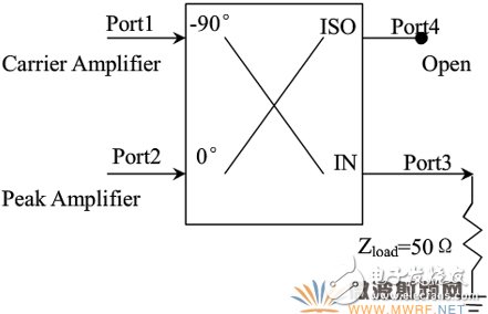
Figure 4, 3dB hybrid bridge port schematic
The S-parameter matrix of the 3dB bridge is
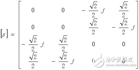
(2)
[b] indicates a reflected wave, [a] indicates an incident wave
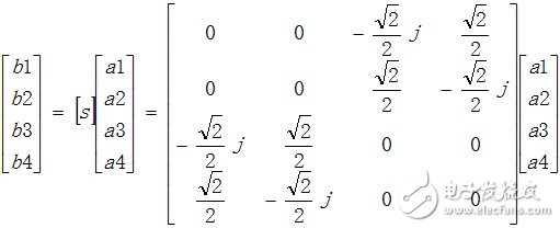
When we open the isolation port, b4=a4, substituting to the above formula, and eliminating b4, a4, we get:
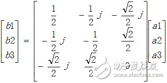
Get a 3-port network, the S-parameter matrix for this 3-port network is
(3)
Comparing with (1), only the phase of the parameters involving the 3 ports is different. If we add the 90° phase shift of the 3 ports of the latter circuit, the S parameter of this circuit is exactly the same as the previous circuit. It is also (1). As shown in Figure 5, the two circuits are equivalent.
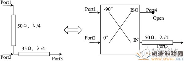
Figure 5, the output of the combined part of the conversion diagram
Since the 3-port combination output is connected to a 50 Ω load, the 50 Ω microstrip on the 3-port amplifier has no effect other than the phase delay.
If we take a 4-port microstrip and open it again, what would be the case? We can reflect the reflection of ports 1 and 2 from port 4 to port 1, port 2, and the 4 ports of microstrip increase the reflection. Path, a path can be moved to ports 1 and 2. Thus, the following two circuits are equivalent and it can be verified that their S-parameter matrix is ​​the same, as shown in Figure 6.
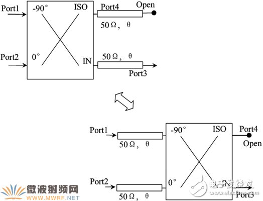
Figure 6, 3dB bridge equivalent conversion
In other words, we adjust the length of the four reflective lines is equivalent to adjust the microstrip length before the combiner, and 4 ports can also short circuit (equivalent to increase the λ / 4 length of the open line) or use capacitors to adjust, different The capacity can be equivalent to different microstrip lengths. Since the Doherty power amplifier needs to carefully adjust the length of the microstrip before the bifurcation combiner, this structure only needs to change the reactance of the isolator port, so the Doherty power amplifier adjustment using the hybrid bridge output combiner is more convenient. The overall transformation relationship is shown in Figure 7.
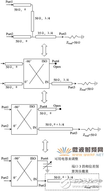
Figure 7, a complete conversion diagram of a 3dB hybrid bridge
4. Improved Doherty Power Amplifier Simulation VerificationWe use the 10W LDMOS power amplifier BLF6G21-10G provided by DXY and perform simulation on ADS by comparing its power and efficiency in the CLASS AB state with the power and efficiency after adopting the improved Doherty structure. Verify the feasibility of the program.
1) Simulation in single-tube CLASS AB state
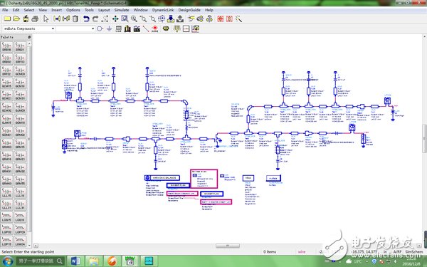
Figure 8, single-tube CLASS AB simulation schematic
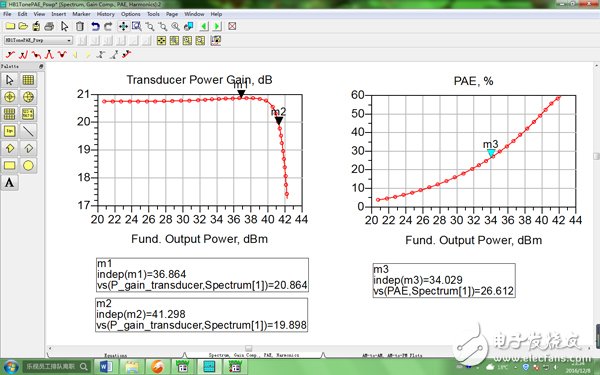
Figure 9. Single-tube CLASS AB simulation results
From the above figures 8 and 9, it can be seen that in the CLASS AB state, the BLF6G21-10G has a P1dB power of 41.3dBm, which is about 12W, and when its output power is 34dBm, the power added efficiency (PAE) is 26.6%.
2) Two-pipe improved Doherty circuit structure simulation
Take two BLF6G21-10G and combine the HC2100A03 3dB hybrid bridge provided at the input and output ends by two DXY cores. One is defined as the main amplifier (carrier amplifier), works in the CLASSAB state, and the other is defined as the peak amplifier. Working in the CLASSC state constitutes the Doherty structure. The simulation process and results are shown in Figure 10 and Figure 11.
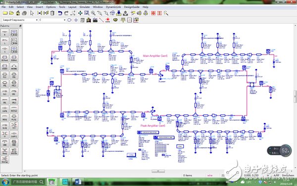
Figure 10: Improved Doherty Simulation Schematic
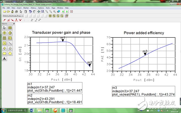
Figure 11. Improved Doherty Simulation Results
From the simulation results in Fig. 11, the peak power of the improved Doherty circuit reaches 43.3dBm, and the output efficiency reaches 43% when the output power is 37.3dBm. Compared with the CLASS AB state, the efficiency is improved when the power backoff is also 6dB. 16.7%.
5 ConclusionBy deducing from the principle, the feasibility of the scheme was demonstrated in theory, and then simulated by ADS. The correctness of the scheme was again obtained from the simulation results. In traditional Doherty circuits, the length of the compensation line needs to be adjusted for both the carrier and the peak circuit. It is difficult to debug complex circuits and is not conducive to mass production. The improved Doherty and CLASS AB circuits are basically the same, simple structure, good reliability, easy mass production, and efficiency has also been greatly improved, is very suitable for WCDMA, CDMA2000, TDD-LTE and LTE-FDD and other mobile The application of communication base stations and repeaters, and subsequently we will also conduct producibility verification by producing actual products at DXY.
Optical Rotary Sensor,Custom Encoder,Optical Encoder 6Mm Shaft,Handwheel Pulse Generator
Jilin Lander Intelligent Technology Co., Ltd , https://www.jilinlandermotor.com