The number of digital designers and digital circuit board design experts in the engineering field is constantly increasing, which reflects the development trend of the industry. Although the emphasis on digital design has brought about major developments in electronic products, it still exists, and there will always be some circuit designs that interface with analog or real environments. Wiring strategies in the analog and digital fields have some similarities, but when you want to get better results, because of their different wiring strategies, simple circuit wiring design is no longer the optimal solution. This article discusses the basic similarities and differences between analog and digital wiring in terms of bypass capacitors, power supply, ground wire design, voltage errors, and electromagnetic interference (EMI) caused by PCB wiring.
Similarities between analog and digital wiring strategies
Bypass or decoupling capacitorWhen wiring, both analog devices and digital devices need these types of capacitors, and both need to connect a capacitor close to its power supply pin. The value of this capacitor is usually 0.1mF. Another type of capacitor is required on the power supply side of the system, usually the value of this capacitor is about 10mF.
The location of these capacitors is shown in Figure 1. The capacitance range is between 1/10 and 10 times the recommended value. But the pin must be short and as close as possible to the device (for 0.1mF capacitor) or power supply (for 10mF capacitor).
Adding bypass or decoupling capacitors on the circuit board and the location of these capacitors on the board are common sense for digital and analog designs. But interestingly, the reasons are different. In analog wiring design, bypass capacitors are usually used to bypass high-frequency signals on the power supply. If bypass capacitors are not added, these high-frequency signals may enter sensitive analog chips through the power supply pins. Generally speaking, the frequency of these high-frequency signals exceeds the ability of analog devices to suppress high-frequency signals. If the bypass capacitor is not used in the analog circuit, noise may be introduced in the signal path, and more serious cases may even cause vibration.
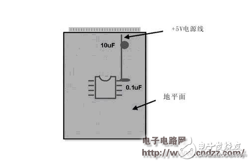
Figure 1 In analog and digital PCB design, bypass or decoupling capacitors (1mF) should be placed as close to the device as possible. The power supply decoupling capacitor (10mF) should be placed at the power cord entrance of the circuit board. In all cases, the pins of these capacitors should be short
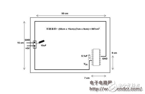
Figure 2 On this circuit board, different routes are used to route the power and ground wires. Due to this improper cooperation, the electronic components and circuits on the circuit board are more likely to be subject to electromagnetic interference.
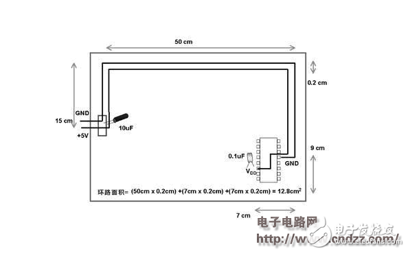
Figure 3 In this single panel, the power and ground wires to the components on the circuit board are close to each Other. The matching ratio of the power line and the ground line in this circuit board is appropriate as shown in Figure 2. The probability of electronic components and circuits in the circuit board being subjected to electromagnetic interference (EMI) is reduced by 679/12.8 times or about 54 times
For digital devices such as controllers and processors, decoupling capacitors are also required, but for different reasons. One function of these capacitors is to act as a "miniature" charge bank. In digital circuits, a large amount of current is usually required to perform the switching of the gate state. Since switching transient currents are generated on the chip during switching and flow through the circuit board, it is advantageous to have additional "spare" charges. If there is not enough charge when performing the switching action, the power supply voltage will change greatly. Too much voltage change will cause the digital signal level to enter an indeterminate state, and may cause the state machine in the digital device to operate incorrectly. The switching current flowing through the circuit board trace will cause the voltage to change, and the circuit board trace has parasitic inductance. The voltage change can be calculated by the following formula: V = LdI/dt
Among them, V = voltage change; L = circuit board trace inductance; dI = current change through the trace; dt = current change time.
Therefore, for many reasons, it is better to apply bypass (or decoupling) capacitors at the power supply or at the power supply pins of active devices.
The power cord and the ground wire should be routed togetherThe position of the power cord and the ground wire are well matched to reduce the possibility of electromagnetic interference. If the power line and the ground line are not properly matched, a system loop will be designed, and noise will likely be generated. Figure 2 shows an example of a PCB design where the power line and the ground line are not properly matched.
On this circuit board, the designed loop area is 697cm2. Using the method shown in Figure 3, the possibility of radiated noise on or outside the circuit board inducing voltage in the loop can be greatly reduced.
The difference between analog and digital wiring strategies
Ground plane is a problemThe basic knowledge of circuit board wiring applies to both analog and digital circuits. A basic rule of thumb is to use an uninterrupted ground plane. This common sense reduces the dI/dt (current change over time) effect in digital circuits, which changes the ground potential and causes noise to enter analog circuits. The wiring techniques for digital and analog circuits are basically the same, with one exception. For analog circuits, there is another point to note, which is to keep the digital signal lines and loops in the ground plane as far away from the analog circuits as possible. This can be achieved by connecting the analog ground plane separately to the system ground connection end, or placing the analog circuit at the farthest end of the circuit board, which is the end of the line. This is done to keep the signal path from external interference to a minimum. This is not necessary for digital circuits, which can tolerate a lot of noise on the ground plane without problems.
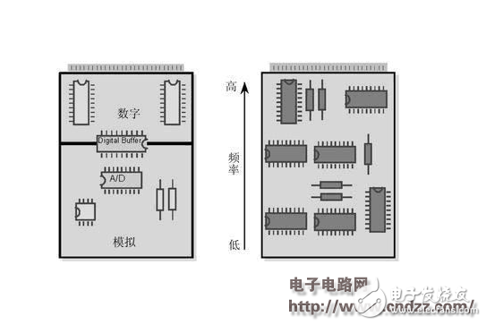
Figure 4 (left) isolates the digital switching action from the analog circuit, and separates the digital and analog parts of the circuit. (Right) To separate the high frequency and low frequency as much as possible, the high frequency components should be close to the connector of the circuit board
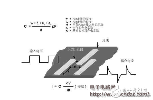
Figure 5 Placing two traces close together on the PCB can easily form parasitic capacitance. Due to the existence of this kind of capacitance, a rapid voltage change on one trace can generate a current signal on the other trace
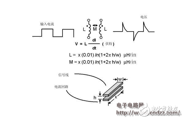
Figure 6 If you do not pay attention to the placement of the traces, the traces in the PCB may produce line inductance and mutual inductance. This parasitic inductance is very harmful to the operation of circuits containing digital switching circuits
Component location
As mentioned above, in every PCB design, the noise part of the circuit and the "quiet" part (non-noise part) should be separated. Generally speaking, digital circuits are "rich" in noise and are insensitive to noise (because digital circuits have a larger voltage noise tolerance); on the contrary, the voltage noise tolerance of analog circuits is much smaller. Of the two, analog circuits are the most sensitive to switching noise. In the wiring of a mixed-signal system, these two circuits should be separated, as shown in Figure 4.
Parasitic components generated by PCB designIt is easy to form two basic parasitic elements that may cause problems in PCB design: parasitic capacitance and parasitic inductance. When designing a circuit board, placing two traces close to each other will generate parasitic capacitance. You can do this: On two different layers, place one trace on top of the other; or on the same layer, place one trace next to the other, as shown in Figure 5. In these two trace configurations, the change in voltage over time (dV/dt) on one trace may cause current on the other trace. If the other trace is high impedance, the current generated by the electric field will be converted into voltage.
Fast voltage transients most often occur on the digital side of the analog signal design. If the trace with fast voltage transients is close to the high-impedance analog trace, this error will seriously affect the accuracy of the analog circuit. In this environment, analog circuits have two disadvantages: their noise tolerance is much lower than that of digital circuits; and high-impedance traces are more common.
Using one of the following two techniques can reduce this phenomenon. The most commonly used technique is to change the size between the traces according to the capacitance equation. The most effective size to change is the distance between the two traces. It should be noted that the variable d is in the denominator of the capacitance equation. As d increases, the capacitive reactance will decrease. Another variable that can be changed is the length of the two traces. In this case, the length L decreases, and the capacitive reactance between the two traces will also decrease.
Another technique is to lay a ground wire between these two traces. The ground wire is low-impedance, and adding another trace like this will weaken the interfering electric field, as shown in Figure 5.
The principle of parasitic inductance in the circuit board is similar to that of parasitic capacitance. It is also to arrange two traces. On two different layers, place one trace on top of the other trace; or on the same layer, place one trace next to the other, as shown in Figure 6. In these two trace configurations, the current on a trace changes with time (dI/dt). Due to the inductance of this trace, voltage will be generated on the same trace; and due to the existence of mutual inductance, it will A proportional current is generated on the other trace. If the voltage change on the first trace is large enough, interference may reduce the voltage tolerance of the digital circuit and cause errors. This phenomenon does not only occur in digital circuits, but this phenomenon is more common in digital circuits because of the large instantaneous switching currents in digital circuits.
To eliminate potential noise from electromagnetic interference sources, it is best to separate "quiet" analog lines from noisy I/O ports. To try to achieve a low-impedance power and ground network, the inductance of the digital circuit wire should be minimized, and the capacitive coupling of the analog circuit should be minimized.
ConclusionAfter the digital and analog ranges are determined, careful routing is essential to a successful PCB. Wiring strategy is usually introduced to everyone as a rule of thumb, because it is difficult to test the ultimate success of the product in a laboratory environment. Therefore, although there are similarities in the wiring strategies of digital and analog circuits, it is still necessary to recognize and take seriously the differences in their wiring strategies.
Portable radios,Motorola Two Way Radios,Motorola Talkabout Radios,Motorola Handheld Radio
Guangzhou Etmy Technology Co., Ltd. , https://www.gzdigitaltalkie.com