A decoder refers to a logic circuit with a decoding function. Decoding is the reverse process of encoding. It can translate a binary code into a signal that represents a certain meaning (that is, a certain state of the circuit) to represent its original meaning. The decoder can be divided into two types: variable decoding and display decoding.
Decoding is the reverse process of encoding. It is the translation of a combination of code into a specific output signal.
classification:
(1) binary decoder, also known as n-2n line decoder
The combination of n inputs is translated into 2n circuit states. Also called n---2n line decoder.
Decoder input: a set of binary codes
Decoder output: A set of high and low level signals
(2) Two-decimal decoder
Direct output binary numbers, people are not accustomed to, can use two-decimal decoder to solve.
This decoder has four inputs and ten outputs.
(3) Display decoder
In digital measuring instruments and various digital systems, the digital quantity needs to be visually displayed, on the one hand, for people to directly read the measurement and calculation results; on the other hand, it is used to monitor the working condition of the digital system.
The block diagram of the digital display circuit is shown below.
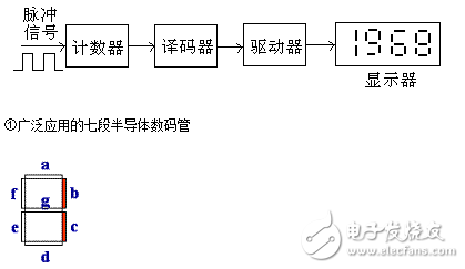
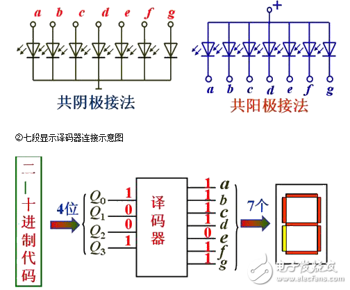
Two digital semiconductor tube connection:
Three basic decoders
In the basics of the decoder, the basic working principle of the full decoder (n-2n) is explained, namely: when the enable terminal is active:
Yi = mi or
/Yi = ! Mi (Note: This indicates the non-number)
In addition to the full decoder, there are 4-10 line decoders and 7-segment display decoders, which are relatively simple. Here's a brief introduction:
- 4-10 decoder
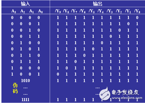
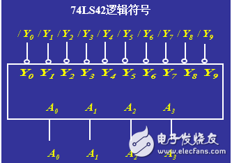
It can be seen from the truth table that when the value of A3A2A1A0 is [0000~1001], the output is valid and all other conditions are invalid. The corresponding logic device diagram is shown in the following figure:
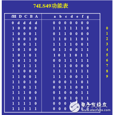
Seven-segment display decoder
Seven-segment display decoder is generally used for LCD or LED display, display 0~9 digital (decimal) or 0~F digital (hex). The so-called seven segments, which represent 0~9 or 0~F, can be displayed by seven digital tubes. The corresponding figure is:
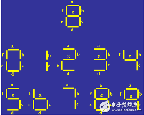
The corresponding truth table is shown in the figure below:
Decoder application
The decoder is mainly used for address decoding, instruction decoding and logical expression representation. The following explanation focuses on how to address memory and how to express logical expressions.
Memory addressing
In the article “Combination Circuits, Sequential Circuits in the Course of Computersâ€, the execution flow of an executable program is explained. The program counter (PC) stores the instructions that the CPU will execute, and how to locate the memory in memory. What is the memory address where the instruction is located? (Focus to understand: This is a hardware implementation, we have to use a combination of circuit addressing).
The following figure describes the memory addressing of the earlier 8086. (The computer uses three types of buses: data bus, address bus, and control bus for data transfer, data bus for data transfer, address bus for transfer address, and control bus for transmitting control signals. Three types of buses are used for IO, Data transfer between memory, CPU and peripherals; each block has several input and output rd, wr, adder, cs, and data, where rd indicates read memory, wr indicates write memory, adder is explained below, cs ( Chip select) means chip select, data is used for data transfer between memory and bus)
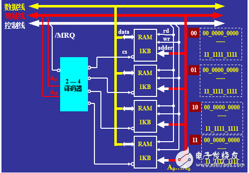
In the 8086 machine, the memory is only 4KB (limited by the current production process, 4KB memory consists of 4 blocks of 1KB memory blocks), and the address is represented by a 12-bit binary string. For each block of 1KB of memory, its addressing range is [00 0000 0000~11 1111 1111]. To address all 4 blocks of memory, the general idea is to share the memory address of the lower 10 bits (A9A8A7A6A5A4A3A2A1A0). Use A11A10 to control it to satisfy:
- When A11A10 = 00, the first block of memory is selected (viewed from above). The range expressed by A11A10A9A8A7A6A5A4A3A2A1A0 is [0000 0000 0000 ~ 0011 1111 1111]
- When A11A10 = 01, the second block of memory is selected (from the top down). The range expressed by A11A10A9A8A7A6A5A4A3A2A1A0 is [0100 0000 0000 ~ 0111 1111 1111]
- When A10A10 = 01, the third block of memory is selected (from the top down). The range expressed by A11A10A9A8A7A6A5A4A3A2A1A0 is [1000 0000 0000 ~ 1011 1111 1111]
- When A11A10 = 11, the fourth block of memory is selected (from the top down). The range expressed by A11A10A9A8A7A6A5A4A3A2A1A0 is [1100 0000 0000 ~ 1111 1111 1111]
Obviously, the above address is really the address we need to express, the rest is how to use the high two A11A10 to control the choice of that 1K memory block. Naturally, the 2-4 decoder can be completed exactly. Therefore, the output of the 2-4 decoder is respectively connected to the chip select signal on each block of 1k memory block, and the above memory addressing function can be realized. (Adder is used to synthesize A11A10 and A9A8A7A6A5A4A3A2A1A0 to make up a 12-bit address)
Decoder expression logic expression
In the decoder, if the enable terminal is valid, the corresponding relationship between the input and output is:
Yi = mi or
/Yi = ! Mi (Note: This indicates the non-number)
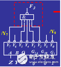
More sensitive children's shoes are easy to find, and there is a relationship between the decoder and the smallest item. For any logical expression, it can be represented by the smallest term, such as F(A,B,C)=m2+m3+m4+m5+m7.
According to /Yi =! Mi, you can further express F(A,B,C) as:
F(A,B,C) = ! (!m2 * !m3 * !m4 * !m5* !m7) (Note: Morgan's Law)
F(A,B,C) = ! (/Y2*/Y3*/Y4*/Y5*/Y7)
At this time, connect the output of 3-8 decoder/Y2, /Y3, /Y4, /Y5 and /Y7 to a NAND gate to express the above logical expression F(A,B,C). The corresponding circuit diagram is shown below:
Based on the above example, how to use a 74LS138 decoder to achieve a totalizer? Before designing, the function of the subtractor needs to be clarified first. Its true value is shown in the following figure:
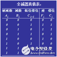
In the subtractor, Ci-1 represents the borrow from the lower position, Ci represents the borrow from the upper position, and Fi represents the calculated value of this position.
According to the truth table, it is easy to get:
Fi = m1 + m2 + m4 + m7
Ci = m1 + m2 + m3 + m7
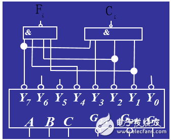
According to the relationship in 74LS138: /Yi = ! Mi, get:
Fi = ! /Y1 + ! /Y2 + ! /Y4 + ! /Y7 = ! (/Y1*/Y2*/Y4*/Y7) (Note: Morgan's Law)
Ci = ! /Y1 + ! /Y2 + ! /Y3 + ! /Y7 = ! (/Y1*/Y2*/Y3*/Y7) (Note: Morgan's Law)
The above-mentioned Fi and Ci have been mapped to the output port of the 74LS138. The output port is connected to the NAND gate to complete the full-subtractor. The corresponding circuit diagram is shown in the following figure:
Stud Triac is developed on the basis of common thyristors. It can not only replace two thyristors with reverse polarity in parallel, but also requires only one trigger circuit and is an ideal AC switch device. . Its English name TRIAC is the meaning of the triac.
China leading manufacturers and suppliers of Stud Triac,Ir Stud Triac, and we are specialize in Stud Type Triac,Sc108 Data Triac Stud, etc.

Stud Triac,Ir Stud Triac,Stud Type Triac,Sc108 Data Triac Stud
YANGZHOU POSITIONING TECH CO., LTD. , https://www.pst-thyristor.com