In order to increase the output speed of display data without increasing the hardware cost, based on the analysis of the existing strip LED display unit board circuit, an LED display control system based on multi-port serial flash memory is proposed. The system consists of STC12C5616. High-speed 1T microcontroller and SST26VF016B serial multi-port flash memory with SPI interface. When displaying the data output, the display data in the multi-port serial flash memory is directly output to the ultra-long strip LED by "memory direct access (DMA)" using the high-speed synchronous serial port (SPI) high-speed clock of the microcontroller. Display. Finally, a 4 096 × 64 dot matrix monochrome LED display was tested as an example. The results show that the display refresh rate reaches 62.5 Hz, which verifies the effectiveness and feasibility of the system in practical applications.
In LED display applications, the ultra-long strip LED screen is a very broad form that is characterized by a "extra long" length and a narrow width. The ultra-long LED display is currently not clearly defined, and it is appropriate to define the number of points in the horizontal direction as ≥2 048.
For example, when the number of points in the horizontal direction is 2 048, the horizontal physical size is 20. 48 m. LED screen. The width (vertical direction) points are generally 16, 24 and 32 points, up to 64 points, and the application is mainly based on Chinese characters that can display a line of various fonts. In order to ensure the refresh rate, in the control of the ultra-long LED display, it is required to send more data within the specified time, and the ordinary LED display control card is difficult to achieve the control requirements.
Based on the analysis of the existing strip LED panel unit circuit, this paper proposes an LED display control system based on multi-port serial flash memory. The controllable clock is generated by the SPI interface of the single-chip microcomputer, and the display data in the multi-port serial flash memory is directly outputted to the super long strip LED display in the "DMA" mode.
1 Common serial board internal serial shift register connection method
Figure 1 shows the internal serial shift register connections for three common cell boards. Figure 1 (a) shows the dot-matrix connection relationship between the unit board 74HC595 and the LED tube and a simplified representation circuit. The serial shift register used inside the LED display unit board is generally 74HC595, MBI5026 or MBI5026 compatible chip, and the MBI5026 can be regarded as a cascade of two 74HC595. It is a constant current source driving mode and is more suitable for LED driving.
Figure 1 (b), (c), (d) are the connection methods of P10, P16, F3. 75 or F5. 0 cell boards respectively.
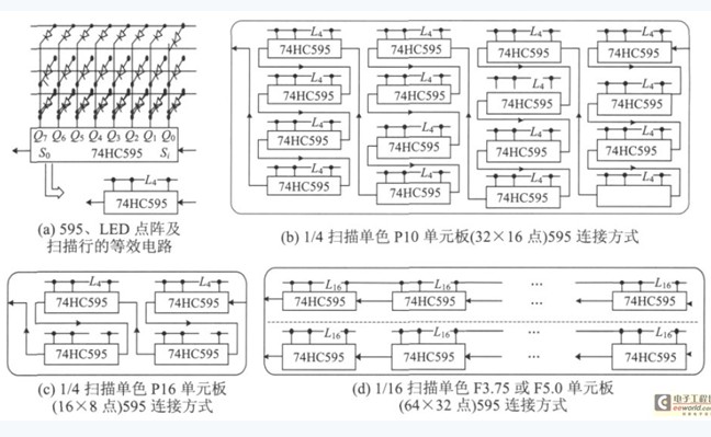
Figure 1 3 common cell board internal serial shift register connection
2 Problems and solutions for ultra-long LED display
At present, a large number of door screens (bar LED displays) on the market are the most widely used form of LED displays. Technically, the horizontal direction of the door screen is from 256 points to thousands of points, and the height generally does not exceed 64 points. As market demand and display accuracy increase, the demand for ultra-long LED displays of thousands of points is increasing. Ordinary LED display control cards are difficult to meet the refresh rate requirement. For example, the F3. 75 LED display with a pixel count of 4 096 in length has a refresh rate of 60 Hz and a SCK clock period of at least 106 /60 / 16 /4 096 = 0. 254 μs = 254 ns.
There are two ways to solve the data output of the ultra-long LED display: First, select high-performance embedded processor and FPGA chip, the method has higher control card cost; Second, skillfully apply special features on the microcontroller and optimize the organization data algorithm This method is very low cost. In this paper, the second method is adopted. The data is pre-written into the multi-port serial flash memory SST26VF016B by the optimization algorithm, and the high-speed controllable SCK clock is generated by the SPI component of the STC12C5616 microcontroller to display the data in the multi-port serial flash memory. Directly output to the ultra-long strip LED display in "DMA" mode to meet the display requirements of the ultra-long LED display.
The ultra-long LED display height generally does not exceed 64 points. If the 1/16 scan monochrome display is controlled, the 4-bit data port of the SST26VF016B memory just meets the data display port width of the LED display. Figure 2 shows the control timing of the SST26VF016B memory. CS is the chip select terminal of the SST26VF016B memory. All operations on the memory are performed while CS is low. SCK is the clock line. When in the idle mode, the SCK signal can be low. The flat state (MODE 0) can also be in a high state (MODE 3); SIO (3: 0) is a 4-bit data port. When data is transmitted, the upper 4 bits of the byte are transmitted first, and then the byte is transmitted. The lower 4 digits. As can be seen from the control timing of the memory, the control of the memory is transmitted in the order of the command word, the 24-bit memory address, the dummy byte, and the data byte 0 to the data byte N. The memory command word can realize the functions of chip erasing, sector erasing, single-byte reading and writing, continuous byte reading and writing, etc., which can fully meet the requirements of the memory capacity and control mode of the ultra-long LED display.
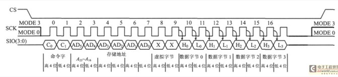
Figure 2 SST26VF016B memory control timing.
The STC12C5616 is a high-speed 1T microcontroller from STC that has a clock frequency of more than 30 MHz and integrates a high-speed serial communication interface component (ie, SPI interface). When the SPI part of the STC12C5616 is operating in master mode, its SPI clock output frequency (fclk) can be up to 1â„4 times the crystal frequency (fosc), and its clock phase and clock polarity can be flexibly configured to satisfy both the SST26VF016B memory. The requirements of the control meet the clock requirements of the ultra-long LED display.
3 ultra long LED display control card circuit design
The multi-bit data port memory of the serial flash memory SST26VF016B and the SPI part of the STC12C5616 microcontroller can generate high-speed SCK clocks, bypassing the display data from the serial flash memory to the LED display. The circuit is shown in Figure 3.
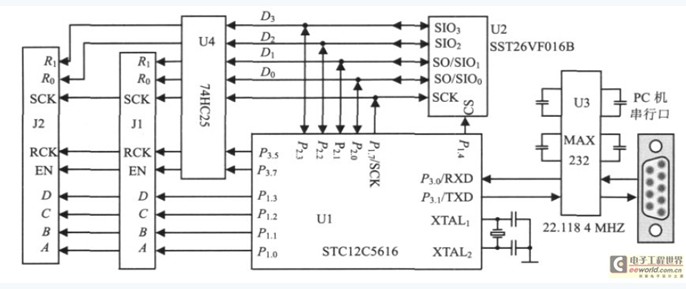
Figure 3 Circuit diagram of the ultra-long LED display control card.
When the dynamic refresh rate of the display reaches 50 times/s, on a 1 / 16 scan LED display, the display time of one line is less than 1 / 50 / 16 s, which is 1. 25 ms. In the control card design, when At fosc =22 MHz, the serial flash clock frequency fclk = 1 /4 fosc =5. 5 MHz, so the time required for 4 096 CLK clocks is 4 096 × 1 /( 5. 5 × 10⁶ ) s = 0. 744 Ms, plus the time to send the memory instruction and address using SQI protocol is less than 1.25 ms, so in Figure 3, the external clock of the microcontroller STC12C5616 selects 22 MHz clock, which can guarantee 4 096 super in SQI protocol mode. Long display display.
The external clock of the single-chip STC12C5616 is selected to be 22.118 4 MHz, which is convenient for the precise control of the serial port baud rate. The pins P3. 0 and P3. 1 are UART interfaces, and the control interface chip and the PC are realized by the communication interface chip MAX232 chip. The communication connection; pin P2. 0 ~ P2. 3 is a 4-bit data line, which is connected to the 4-bit data port of the memory SST26VF016B on the one hand, and connected to the data line of the output interface of the LED unit board by the 74HC245 on the other hand. on. There are 2 monochrome LED unit board output interfaces on the control card, interface J1 uses data lines D0 and D1, interface J2 uses data lines D2 and D3; pin P1. 7 is SPI clock output, and SPI clock output lines are connected at the same time. The clock input to the serial flash memory SST26VF016B and the LED unit board; pin P1. 4 is the chip select signal of the serial flash memory SST26VF016B; pin P3. 5 is the data latch signal of the LED unit board; pin P3. 7 It is the enable signal output of the LED unit board; pins P1. 0 ~ P1. 3 are the row selection signal output of the LED unit board; J1 and J2 connectors are used to connect the LED unit board of the display in the height direction to match The door screen has a height requirement of 64 points.
The circuit is designed to flexibly implement three different data access modes between the microcontroller, serial memory, and LED cell board:
(1) Normal access between the microcontroller and the memory.
As can be seen from Figure 3, the connection between the microcontroller STC12C5616 and the serial flash memory SST26VF016B is connected with reference to the data sheet, which can achieve normal data access, and the data will also enter the shift register buffer on the LED unit board. Zone, but as long as the data latch RCK on the LED unit board does not get a valid signal, the data entering the LED unit board is invalid data that is not displayed.
(2) Data communication between the microcontroller and the LED unit board.
Set the MCU pin P1. 4 to the high level, that is, the enable end of the serial flash memory is invalid. At this time, the data port of the memory is in a high-impedance state, and the data communication between the MCU and the LED cell board is not affected by the memory data port. The effect of the microcontroller's data can be output to the LED unit board.
(3) Data transfer between the memory and the LED display.
First adopt the (1) mode, the MCU first outputs the command word, the memory address and the dummy byte to the serial memory, and then sets the data ports P2. 0 ~ P2. 3 of the MCU all high, through the SPI clock from the string. The line memory reads the display data and enters the LED unit board in the "DMA" mode. After reading a line of data, a valid signal is generated on the data latch terminal RCK on the LED unit board, and the line data can be displayed. When using this mode, be sure to set the pins P2. 0 ~ P2. 3 of the microcontroller STC12C5616 to the "weak pull-up" mode.