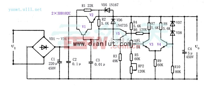
Below is the circuit diagram of a practical high-voltage DC power supply.
This is a practical high-voltage DC regulated power supply circuit designed for real-world applications. In many industrial settings, long-term stable high-voltage DC power supplies are essential. However, conventional voltage regulator circuits often struggle to meet these demands due to limited dynamic range and poor stability. To overcome this, the design incorporates a differential circuit as the sampling and comparison stage of the regulator, significantly improving the output dynamic range—up to around 100V. The prototype was tested and performed exceptionally well, meeting the following specifications:
Input AC: 150V ~ 250V; Output DC: 150V - 250V, with excellent stability across all values. The power supply exhibits minimal sensitivity to ambient temperature and low power consumption, making it ideal for continuous operation. The schematic is shown in the figure below, along with a brief explanation of its working principle.
The 220V AC input is first rectified by a bridge rectifier (VD1–VD4). After filtering through capacitors C1 and C2, a DC voltage of approximately 330V is generated between the collector of the composite adjustment tube and ground. This voltage is further regulated using a pre-regulation circuit composed of resistor R1 and Zener diode VD5, allowing the output to stabilize at 150V–250V DC.
In the circuit, VD5–VD8 are Zener diodes with different voltage ratings, each contributing to voltage regulation within their respective sections. VD5 and R1 form a pre-regulator that provides a stable reference voltage to the base of V2, ensuring that the composite transistor (V1 and V2) remains forward-biased. This helps reduce output voltage fluctuations and improves the regulation rate and output impedance. VD6 clamps the emitter voltage of V5, preventing excessive Uce5, thus addressing the voltage withstand issue of V5. VD7 and VD8, which have opposite temperature coefficients, help minimize the impact of temperature changes on the output. Together, they also serve as the final voltage regulation stage.
V2 and V1 are high-power transistors that form a composite transistor, acting as the core component of the power supply. C3 is a ceramic capacitor used to suppress oscillations. To further enhance stability and achieve a wide output dynamic range, a differential amplifier is used as the sampling and comparison circuit. This ensures better voltage regulation that is less affected by temperature variations. The regulation process works by detecting any change in output voltage via the differential amplifier, generating a control signal that adjusts the CE voltage of V2 and V1, pulling the output back to the desired level.
A potentiometer RP1 is mounted on the panel to allow manual adjustment of the output voltage. RP2 is used during debugging to fine-tune the dynamic range. Once set, RP2 should not be moved again and can be sealed with glue for stability. While the rest of the components can be selected based on the schematic, special attention is given to the selection of V1 and V2. Given the requirement of U0 = 150V–250V and I0 ≤ 50mA, the maximum Uceo for V1 and V2 is calculated as approximately 220V, with a maximum power dissipation of 11W. In practice, a pair of 3DD102C transistors were chosen for this purpose.
Battery Charger,Ac/Dc Charger,Lithium Charger,Lithium Ion Charger
ShenZhen Yinghuiyuan Electronics Co.,Ltd , https://www.yhypoweradapter.com