background
Perhaps, you will think that the DPDK (Data Plan Development Kit) is a high-speed data transmission standard applied at the network application layer; perhaps, you think that the DPDK is a set of specifications developed by Intel; perhaps, you think that the DPDK is in the CPU and ASIC world. Limited confidentiality; or perhaps, you have never heard of DPDK, considering its history, it is very likely. So, if one of the above assumptions is correct, then you should read the following.

Initially, the DPDK was a data layer library set. Later, Intel developed a driver for the Intel X86 microprocessor that can quickly process the NIC (Network Interface Control). This is the past life of the DPDK. The DPDK in this life has been a Linux fund project in April last year and can be seen on DPDK.org.
The DPDK mainly includes the following main libraries that are commonly used:
Send and receive data packets when it is necessary to minimize the number of CPU cycles (generally less than 80);
Develop a fast grouping algorithm;
Run a third-party shortcut path stack.
So far, the DPDK sounds like a special web development tool, but as Atomic Rules's CTO Shep Siegel said: "If you can make your data transfer problem look like a packet transmission problem, Then, in your development process, DPDK may be a more helpful shortcut."
Arkville
And, more details about the recent DPDK, Siegel's team may know more, mainly because his team just released Arkville, which is a DPDK-enabled FPGA/GPP data transfer IP block and DPDK PMD (Poll Mode Driver) Collaborate with the Linux Fund Open Source DPDK Library 17.05 release to allow the Linux DPDK application to offload the server to the FPGA gate). At the same time, the Arkville distribution of Atomic Rules is also compatible with Xilinx Vivado2017.1 (this is the latest version of the Vivado design tool just released in April this year). In addition, Atomic Rules provides two simple demo designs (both compileable with Vivado 2017.1):
4-port, 4-queue 10GbE demo (Arkville + 4 x 10 GbE MAC)
Single port single queue 100GbE demo (Arkville + 1 x 100 GbE MAC)
Both of the above examples are data movers. To be precise, Arkville is a packet conduit with a CPU-side DPDK interface, an FPGA-side AXI interface, and a hardware on the Arkville pipeline that can be easily added to handle these packets. Design point, and this is where the CPU shunt logic is.
The Arkville IP developed by Atomic Rules works well with all Xilinx UltraScale devices, but works better with the Xilinx UltraScale+ all-programmable device, thanks to the integration of two PCIe Gen3 x 16 controllers in a fully programmable device ( Includes Kintex UltraScale+ and Virtex UltraScale+ FPGA family devices and Zynq UltraScale+ MPSoC family devices.
why?
As the director of VPCraig Lund of BittWare Enterprise said, "100G Ethernet is not possible, but whether you can achieve this rate by using PCIe on the server side [using a PCIe Gen3 x 16 interface] is not clear. From PCIe In terms of parameters, this may seem simple, but it is not the case." Lund also said that if you are dealing with a minimum size packet, you can do it with a large number of more than 14 million per second. But if you're dealing with a large packet, it will require more bandwidth, which may be a challenge to the productivity of a single PCIe Root complex, but it's really not enough.
Using Atomic Rules' ArkvilleIP, BittWare developed its own product, the XUPP3R PCIe card, and it also combined a Xilinx Virtex UltraScale+ VU13P FPGA chip. One of the many unique features of BittWare's XUPP3R PCIe board is that it has two PCIe Gen3 x 16 ports: one for the edge connector and one for the optional continuous expansion port. The second PCIe Gen3x16 port can be used as a second PCIe slot for increased bandwidth.
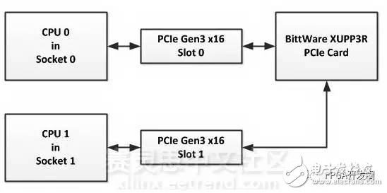
However, although Lund did not say much, here is not only two PCIe Gen3 x 16 slots, but two PCIe Gen2 Root complexes, which means that two sets of slots are required, then two The CPU works to process the data path. The following simplified block diagram illustrates Lund's point of view:
BittWare not only developed the XUPP3R PCIe card with two PCIe Gen3 x 16 ports, but BittWare also developed two products using its XUPP3R PCIe card and Arkville IP:
StreamSleuth, a 100GbE network packet processor.
StreamSurge, a 1U box with an Intel E5 v4 single-socket server and a NIC designed with the XUPP3R PCIe card and BittWare's StreamSurge IP.
However, the need to check the number is: Arkville is an IP provided by Atomic Rules, XUPP3R PCIe card is a product provided by BittWare, the two can not be confused.
to sum up
At present, a large number of data bursts, in addition to firmware transport, the most convenient bus (PCIe / ETH) line transmission, not only high speed and high security, but as the situation develops, its rate requirements are getting higher and higher, expectation Xilinx FPGAs can make more contributions to increasing data transfer rates.
SHENZHEN CHONDEKUAI TECHNOLOGY CO.LTD , https://www.szsiheyi.com