 Fujifilm has released a significant reduction in sensitivity due to changes in the angle of incidence of light (see figure) for CMOS sensors (organic CMOS sensors) using organic photoelectric conversion films under development.
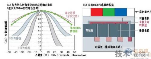
 Achieving Characteristics Close to the Theoretical Limit Since the organic CMOS sensor developed by Fujifilm has almost no incident angle dependence, it has the characteristic (a) that it is easy to suppress the decrease in sensitivity. In order to obtain this characteristic, the structure of the organic CMOS sensor has been improved (b). (Figure: This site is based on Fujifilm's data)
(Note 1) Fujifilm succeeded in capturing monochromatic images using an organic CMOS sensor in 2006 and succeeded in taking color images in 2009.
If a common CMOS sensor using silicon has an incident angle of more than 30°, the output voltage will drastically decrease, compared with no significant voltage drop in this development. Fujifilm stated that this is achieved by "improving the materials and the production process of organic photoelectric conversion films," and the angular dependence of the output voltage has reached the same level as the theoretical limit of the imaging element. As a result, organic CMOS sensors promise to achieve narrower pitches than CMOS sensors using silicon.
Although high-sensitivity CMOS sensors are represented by a backside illumination (BSI) sensor, in practice, there is a limit to the incident angle dependence and narrow pitch. The narrower the spacing, the more severe the crosstalk (mixing) of incident light into neighboring pixels, "BSI sensors with a pixel pitch less than 0.9 μm are quite difficult to achieve" (industry insiders).
In this regard, the organic CMOS sensor developed this time exceeded the limit of the BSI sensor. For example, when the incident angle reaches 40 degrees, about twice the output voltage of the BSI sensor can be obtained. This feature can also be maintained at narrow spacing. This is because the thickness of the organic photoelectric conversion film is only 0.5 μm, and it is difficult for light to enter adjacent pixels.
The remaining problem is to improve the picture quality. At this stage, the reason for deterioration in picture quality is random noise up to 38 electrons (rms value). Fujifilm explained that "the reason is the noise caused by the thermal fluctuations of the charge called kTC noise. Currently, (the company) is working with other companies to develop a solution to the problem by improving the signal processing circuit." If random noise can be suppressed to single-digit electrons, organic CMOS sensors are expected to be put into practical use.
Diode Module is called silicon stack, it is made from several diodes in series, the number of the diode is by its highest pressure (maximum) negative peak pressure, main purpose is for high voltage rectifier. China Diode Module,High Voltage Diodes supplier & manufacturer, offer low price, high quality Caterpillar Diode Module,High Frequency Diode Module, etc.
Diode Module
Diode Module,High Voltage Diodes,Caterpillar Diode Module,High Frequency Diode Module
YANGZHOU POSITIONING TECH CO., LTD. , http://www.yzpst.com