Abstract : Some analog signals are often used in control systems. Usually, digital-to-analog converters are used to output the required analog signals. Computer-controlled digital-to-analog converters require an external bus interface. The USB interface is a commonly used external bus interface that is very convenient for controlling digital-to-analog converters. The author takes a typical USB interface chip and D/A converter chip as an example to illustrate the circuit and program design method of the digital-to-analog conversion system based on USB interface.
0 Preface
In the control system, it is often necessary to generate and control some analog signals, and the commonly used microprocessor external bus interface is a digital signal, which cannot directly generate the required analog signal, which uses a D/A converter. The D/A converter can be controlled via the USB interface to output the required analog voltage or analog current.
As an external bus interface commonly used by microprocessors, the USB interface has been widely used. The USB interface reduces development time, risk and cost, thus achieving the most economical solution in the quickest way.
This paper takes USB interface chip PDIUSBD12 and voltage output type D/A converter chip AD558 as an example, and elaborates the DAC system circuit and program design method based on USB interface.
1 USB interface chip PDIUSBD12 introduction
The USB interface chip selected by this system is the USB1.1 interface chip PDIUSBD12 produced by Philips. It is a cost-effective USB device, which is usually used as a high-speed universal parallel interface for communication with the microcontroller in the microcontroller system. . It also supports local DMA transfers. The main features of the PDIUSBD12 chip are as follows:
· Comply with the USB1.1 specification;
Integrated SIE, FIFO memory, transceiver and voltage regulator;
Fully autonomous direct memory access (DMA) operations;
Integrated 320-byte multi-structure FIFO memory;
· 1MB/s data transmission rate can be achieved in both batch mode and synchronous mode;
· Bus power supply capability with good EMI characteristics;
· Can be connected to USB via software control;
· Has a programmable clock frequency output;
· Meet ACPI, OnNOW and USB power management requirements;
· On-chip electrostatic protection circuit higher than 8kV;
Dual power operation: 3.3±0.3V or extended 5V power supply, ranging from 3.6~5.5V;
All of these features provide significant system cost savings while making USB functionality easy to use on peripherals. Low power consumption allows it to be applied to peripherals powered by the bus.
2 D / A conversion chip AD558 introduction
The DAC chip selected by this system is the 8-bit voltage output type D/A converter AD558 introduced by Analog Devices. The main feature of the voltage output type D/A converter is that there is no amplification part of the delay, which can achieve high speed, but the load. Limited capacity, generally used in high impedance loads.
The basic method used for D/A conversion is to convert digital quantities into binary data. Each of its bits produces a corresponding voltage or current, and the magnitude of this voltage or current is proportional to the weight of the corresponding binary bit. Finally, these voltages or currents are added and output.
A complete D/A converter mainly includes three parts, namely, a weighted resistance decoding network, a digitally controlled electronic switch combination, and a current-voltage converter composed of an operational amplifier. The principle of the D/A converter is shown in Figure 1.
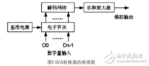
In general, parallel D/A converters have higher digital-to-analog conversion speeds than serial D/A converters. The reason for the fast conversion speed of the parallel D/A converter is that at the input of the digital quantity, each digital bit is simultaneously input to the corresponding port of the converter. The conversion time of the entire device depends on the settling time of the power supply voltage and the summing time of each power bit. These times are generally very short and generally reach the order of nanoseconds or microseconds. Therefore, for high speed requirements, parallel D/A converters should be preferred.
In the AD558 type D/A converter, the electronic switch group corresponds to the input binary numbers D0 to D7. When a binary bit is 1, the corresponding electronic switch is closed, and the reference voltage Vref is connected to the weighted resistance decoding network, so that a current flows through the branch resistance; when a certain binary bit is 0, the corresponding electronic switch is turned off. No current flows through the branch resistor. The resistance value of each branch of the weighted resistance decoding network is inversely proportional to the weight of the input binary data D0~D7. The resistance value of the large weight is small, and the resistance value of the small weight is large. The D/A converter obtains the summed analog voltage value and outputs it according to the condition of each weight and the input binary number through the summation and current-voltage conversion circuit.
In the D/A converter, the number of digits also reflects the resolution of the D/A converter, that is, the change of the corresponding analog output value when the input digital quantity changes by a unit number. For an 8-bit voltage type D/A converter, when the input digital quantity changes in unit, the analog output changes to V/255, where V is the full scale of the voltage output.
The main performance indicators of the AD558 are as follows:
· 8-bit parallel interface;
·The output range of voltage is 0~+10V;
· Relative accuracy ± (1/2) least significant bit;
· Output conversion establishment time 1 s;
· Use a single power supply, the power supply voltage range is +4.5~+16.5V;
·There is a reference voltage source inside, no need for external reference source;
· Internally integrated with data latches;
·75mW low power consumption.
3 circuit design
This system uses the USB control chip PDIUSBD12 and D/A converter AD558 to realize DAC control. The computer can control the various analog signals required for the AD558 output via the USB interface. Since the computer's USB interface has an external power supply function, the power supply of the USB interface is used to power the PDIUSBD12 chip.
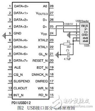
The circuit schematic of the USB interface part is shown in Figure 2.
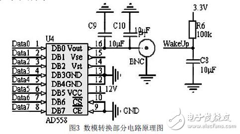
The data bus of the AD558 is connected to the PDIUSBD12.AD558 operating in the 0~+10V analog voltage output mode. Capacitors C9 and C10 are used to improve the output waveform. The AD558 operates from a single 12V supply and does not require an external reference. The circuit schematic of the digital-to-analog conversion section is shown in Figure 3.
When manufacturing PCBs, the requirements for high-speed USB printed circuit boards should be observed. In order to achieve higher signal quality, a 4-layer board or even a 6-layer board is required for wiring. Place the USB chip in the signal layer as close as possible to the GND plane.
D+ and D- in the USB interface are used for high-speed USB data transmission, so these two signal lines directly affect the stability of the USB interface circuit, and need to be carefully arranged when wiring the printed circuit board. The traces of D+ and D- should be as short and equal as possible, and the wire width and spacing of D+ and D- should be properly set. The differential impedance between D+ and D- should be 90W ± 10%. Ensure that the complete GND layer is below the D+ and D- signals. A broken GND layer in the middle will result in a differential impedance mismatch and increase signal interference.
Intelligent Street Lights,Intelligent Track Lighting,Green Intelligent Lighting,Intelligent Led Street Lighting
Jiangsu Bosiwei Optoelectronics Group Co.,ltd , https://www.bswledled.com