This application note outlines the effects of bias timing control requirements and the use of different bias conditions. This application note also describes an optimal solution for biasing RF/microwave amplifiers using active bias controllers such as the HMC980, HMC980LP4E, HMC981, HMC981LP3E, HMC920LP5E, etc.
Bias amplifier
Power sequencing
Power sequencing is very important when using an external bias amplifier for the following reasons:
â— Failure to follow proper power sequencing can affect device stability. Exceeding the breakdown voltage may cause the device to fail immediately. Long-term reliability is reduced when conditions exceeding the boundary conditions occur multiple times and the system is under pressure. In addition, continuous violations of the timing control mode can damage the on-chip protection circuitry and cause long-term damage, resulting in field operation failures.
â— Optimize the bias level not only during power-up and power-down, but also during normal operation, which can improve the performance of the RF amplifier, depending on configuration and application requirements. For some applications, the RF performance of the amplifier can be changed to suit different field conditions. For example, in rainy days, the output power can be increased to widen the coverage, and on a sunny day, the output power can be reduced. The amplifier's external gate voltage control enables these functions.
Analog Devices has a wide range of RF amplifiers. Many RF amplifiers are based on depletion high electron mobility (pHEMT) technology. Transistors used in this process typically require a power supply to power the drain and gate pins. This quiescent drain current is related to the gate voltage. See Figure 1 for typical IV characteristics of a typical field effect transistor (FET) process.
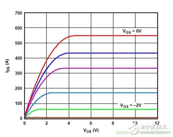
Figure 1. Typical IV characteristics of a typical FET process
As the gate-to-source voltage (VGS) increases, more electrons enter the channel, producing a higher drain-source current (IDS).
In addition, as the drain-source voltage (VDS) increases, the electric field force that pulls the electrons becomes larger, and the drain-source current also increases (in the linear interval).
In practical amplifiers, these amplifiers can be broadly classified into two categories due to effects such as channel length modulation: self-biased amplifiers and external bias amplifiers.
Self-bias amplifier
The self-bias amplifier has an internal circuit to set the optimum bias point for operation. These amplifiers are typically best suited for broadband low power applications. See Figure 2 for a typical pinout of a self-biased amplifier.
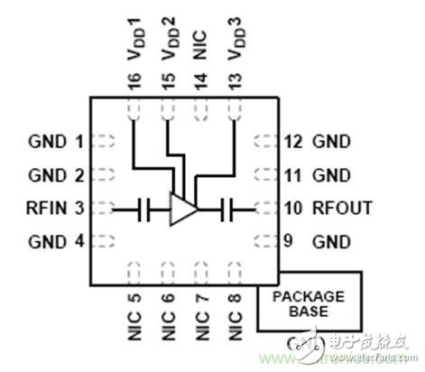
Figure 2. Typical pinout of a multistage self-biased amplifier with multiple bias pins
Self-biased amplifiers, while easy to use, may not provide optimal performance because internal resistive bias circuits do not adequately compensate for batch, device, and temperature differences.
External bias amplifier
External bias amplifiers often provide higher performance than self-biased amplifiers under certain bias conditions. The quiescent drain current of the amplifier affects parameters such as power compression point, gain, noise figure, intermodulation products, and efficiency. For these high-performance external bias amplifiers, proper power sequencing is critical to ensure that the device operates safely at peak performance.
Figure 3 shows a typical connection of the external bias amplifier pins and the corresponding transistor pins. The pin mapping in Figure 3 is a simplified schematic of the amplifier.
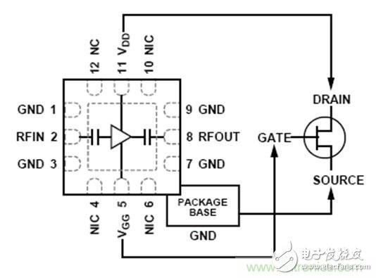
Figure 3. Typical connection of an external bias amplifier
In addition, many external bias amplifiers meet multiple gain, bandwidth, and power requirements through multiple stages. Figure 4 shows a typical block diagram of the multi-stage external bias amplifier HMC1131.
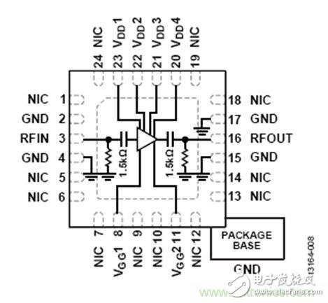
Figure 4. HMC1131 Multistage External Bias Amplifier
HMC1131 bias and timing control requirements
The HMC1131 is a power amplifier for gallium arsenide (GaAs), pHEMT monolithic microwave integrated circuits (MMICs). The operating frequency range is from 24 GHz to 35 GHz. The typical performance offered by this 4-stage design is 22 dB gain, 23 dBm output power (1 dB compression, or P1dB) and 27 dBm saturated output power (PSAT). The corresponding bias conditions are VDD = 5 V and IDQ = 225 mA. Where VDD is the drain bias voltage and IDQ is the quiescent drain current. This information is given in the HMC1131 data sheet for the electrical specification table for the 24 GHz to 27 GHz frequency range. Figure 4 shows the pin connections for the HMC1131.
To achieve a target quiescent drain current (IDQ) of 225 mA, the gate bias pin voltages (VGG1 and VGG2) should be set between 0 V and −2 V. To set this negative voltage without damaging the amplifier, follow the recommended bias sequence during power-up and power-down.
The following is the recommended offset sequence during power-up of the HMC1131:
Connect to the ground.
Set VGG1 and VGG2 to −2 V.
Set the drain voltage bias pins VDD1 to VDD4 to 5 V.
Increase VGG1 and VGG2 to achieve an IDQ of 225 mA.
Apply a radio frequency signal.
The following is a recommended offset sequence during the HMC1131 power down:
Turn off the RF signal.
Reduce VGG1 and VGG2 to −2 V to achieve an IDQ of approximately 0 mA.
Reduce VDD1 to VDD4 to 0 V.
Increase VGG1 and VGG2 to 0 V.
When the gate voltage (VGGx) is −2 V, the transistor is pinched off. Therefore, the typical value of IDQ is close to zero.
In general, the recommended bias sequences for most external bias amplifiers are similar. Different devices will have different IDQ, VDDx, and VGGx values. To turn off the device, VGG for GaAs devices is typically set to −2 V or −3 V, while for gallium nitride (GaN) amplifiers, this voltage can be −5 V to −8 V. Similarly, VDDx for GaN devices can reach 28 V or even 50 V, while GaAs amplifiers are typically less than 13 V.
The VGG pins of a multistage amplifier are typically tied together and biased together. Following the same procedure, the user can get the typical performance results available in the data sheet. Using an amplifier under different bias conditions may provide different performance. For example, using different VGGx levels for the HMC1131 gate bias pin to achieve different IDQ values ​​can change the RF and DC performance of the amplifier.
Figure 5 shows the P1dB vs. frequency for the HMC1131 at different supply currents. Figure 6 shows the output versus third-order intercept point (IP3) performance versus frequency for different supply currents.
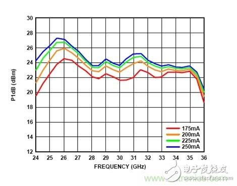
Figure 5. P1dB vs. frequency for different supply currents
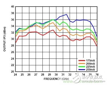
Figure 6. Output IP3 vs. frequency for different supply currents, POUT/sound = 10 dBm
Another option to utilize multiple VGGx pin bias amplifiers is to independently control the gate bias pins. This mode of operation helps the user customize the device by optimizing specific parameters such as P1dB, IP3, NF, gain, and power consumption.
This flexibility is beneficial for some applications. If the performance data provided in the amplifier data sheet can easily meet certain requirements of the application, but is slightly different from other requirements, test under different bias conditions without exceeding the absolute maximum ratings given in the data sheet. Performance may be beneficial.
Another alternative to biasing the external bias amplifier is to set VGGx to achieve the desired 225 mA IDQ and use a constant gate voltage during normal operation. In this case, the IDD of the amplifier will increase under RF drive. For this behavior, see the 30.5 GHz power compression map in the HMC1131 data sheet (shown by the orange line). An amplifier with a constant gate voltage and an amplifier with a constant IDD may improve different performance.
Cascode amplifier
ADI's wideband distributed amplifiers often use a cascode architecture to extend the frequency range. The cascode distributed amplifier uses a fundamental frequency unit consisting of two FETs connected in series, source to drain. The baseband unit is then copied multiple times. This duplication will increase the working bandwidth. Figure 7 shows the schematic diagram of the fundamental frequency unit.
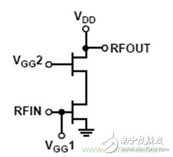
Figure 7. Schematic diagram of the fundamental frequency cascode unit
With some exceptions, cascode wideband amplifiers are typically externally biased.
The HMC637A is a wideband amplifier with a cascode topology. The HMC637A is a GaAs, MMIC, metal-semiconductor field effect transistor (MESFET) distributed power amplifier that operates from DC to 6 GHz. Figure 8 shows the pin connections for the HMC637A.
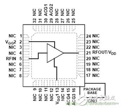
Figure 8. HMC637A pin connection
The amplifier provides 14 dB gain, 43 dBm output IP3, and 30.5 dBm output power (1 dB gain compression) with bias conditions of VDD = 12 V, VGG2 = 6 V, and IDQ = 400 mA. This information is given in the electrical specifications table in the HMC637A data sheet.
To achieve the recommended 400 mA quiescent drain current, VGG1 must be between 0 and −2 V. To set the required negative voltage, follow the recommended bias sequence during power-up and power-down.
The following is a recommended offset sequence during power-up of the HMC637A:
Connect to the ground.
Set VGG1 to −2 V.
Set VDD to 12 V.
Set VGG2 to 6 V (VGG2 is available from VDD through a resistor divider).
Increase VGG1 to achieve a typical quiescent current (IDQ) of 400 mA.
Apply a radio frequency signal.
The following is a recommended offset sequence during the HMC637A power down:
Turn off the RF signal.
Lower VGG1 to −2 V to achieve IDQ = 0 mA.
Reduce VGG2 to 0 V.
Reduce VDD to 0 V.
Increase VGG1 to 0 V.
Bias external bias amplifier with active bias controller
There are two main methods for biasing an external bias amplifier:
â— Constant gate voltage method. This method first achieves the desired IDQ value by changing the gate voltage value. This gate voltage value then remains constant during operation, which typically results in a change in the drain current (IDD) under RF drive.
â— Constant IDD method. This method first changes the gate voltage value to achieve the desired IDQ value, then monitors the IDD value of the amplifier, and continuously adjusts the gate voltage value to have the same IDD value at different RF drive levels. The active bias controller keeps the IDD of the device under test (DUT) constant.
There is also a method which belongs to the constant IDD method, which is as follows: first operates according to the constant IDD method, and then switches between a plurality of constant IDD levels according to the needs of the site specific situation. For example, on rainy days, the user can bias the transmitter's power amplifier stage to achieve high current levels to compensate for additional rain-induced attenuation. On sunny days, the user can bias the power amplifier to achieve low current levels, thereby reducing power consumption.
ADI's RF amplifiers are typically calibrated using a constant gate voltage method and a benchtop power supply unit. Therefore, biasing these amplifiers with a constant IDD method may result in different RF performance than the performance given in the amplifier data sheet.
It can be cumbersome to design an amplifier bias circuit to keep the drain current constant and provide the necessary timing control. This type of control circuit can be complicated, requiring not only multiple external components such as low dropout regulators (LDOs), charge pumps, voltage timing control and protection circuitry, but also calibration cycles. Such implementations typically occupy a much larger printed circuit board (PCB) area than the amplifier itself.
The HMC920LP5E integrates all required work modules in a compact 5 mm &TImes; 5 mm plastic surface mount (SMT) package. Compared to discrete biasing schemes, this compact solution eliminates multiple ICs and external components and thus occupies less PCB area.
Similar to the HMC920LP5E, active bias controllers require less PCB area than discrete transistor solutions. With the HMC980LP4E, bias timing control, constant gate voltage regulation, short-circuit protection, and negative voltage generation are all achieved in a 10 mm & TImes; 15 mm PCB area.
The HMC981LP3E, HMC980LP4E, and HMC920LP5E are 3 mm & TImes; 3 mm, 4 mm & TImes; 4 mm and 5 mm × 5 mm plastic package active bias controllers. Figure 9 shows the PCB area required for a typical application, including external passive components.
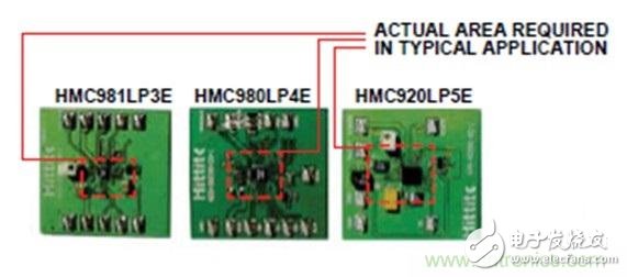
Figure 9. PCB area required for typical applications
ADI's family of active bias controllers offers a number of key benefits:
â— The internal negative voltage generator generates the negative voltage required by the external bias amplifier on the VGATE pin. The presence of these generators eliminates the need for voltage inverters, reducing the number of components, PCB area and system cost.
â— Continuous internal gate voltage adjustment ensures that the DUT drain current is constant.
â— Since the influence of the difference between devices is reduced, the offset accuracy is improved. For different amplifiers of the same device type, the optimum gate voltage level required to achieve the desired IDD is different due to differences between devices. Therefore, setting the same gate voltage value for each DUT will result in different RF performance. The active bias controller adjusts the gate voltage levels of individual DUTs to reduce performance differences caused by differences between devices.
Figures 10 and 11 show the reduction in the effect of differences between devices.
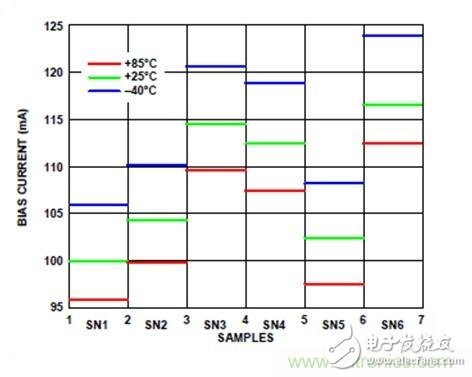
Figure 10. Bias current difference for a typical amplifier with a fixed external VGATE bias
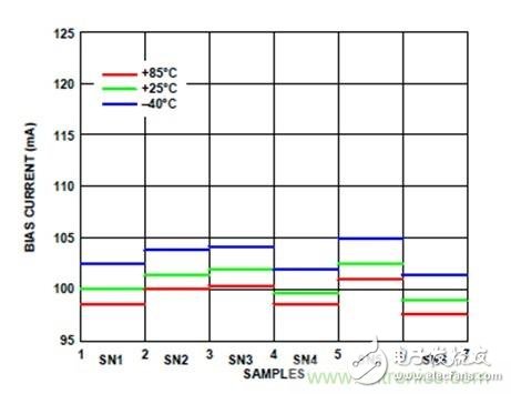
Figure 11. The bias current difference of the same amplifier is improved when biased with the HMC920LP5E
â— The internal bias timing control circuit ensures that the DUT is not supplied with a positive voltage on the VDRAIN pin and the VG2 pin when the VGATE negative voltage is not present. This eliminates the need for external components to perform timing control during power-up and power-down of the DUT.
â— After the VGATE pin, the short-circuit protection circuit disables the VDRAIN pin, ensuring that the DUT is safe even in the event of a short circuit.
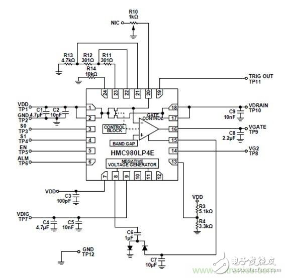
Figure 12. Typical application circuit for the HMC980LP4E
The gate voltage auto-control function uses internal feedback to cause a constant quiescent bias current to flow through the biased amplifier, which is independent of temperature and amplifier threshold changes. The static bias current is adjusted with an external resistor. Figure 12 shows the RSENSE resistor (R10) connected to pin 20 of the HMC980LP4E.
See the Active Bias Controller Data Sheet for more information on how to calculate the RSENSE and VDD values.
Analog Devices offers three active bias controllers: the HMC920LP5E, the HMC980LP4E, and the HMC981LP3E. Table 2 details some of the important features of these active bias controllers.
The HMC980LP4E is capable of delivering high current to the drain, while the HMC981LP3E is best suited for devices that require lower drain current. In addition to the negative voltage generator, the HMC920LP5E also integrates a positive voltage regulator that supplies power to the drain pin.
working principle
For external bias amplifiers, the offset requirements for VGG and IDD are specified at the bottom of the Analog Devices data sheet. For example, the HMC637A requires that its VGG1 be adjusted from −2 V to 0 V to obtain an IDQ with a typical value of 400 mA. However, the recommended power-up and power-down sequences should be followed to avoid damage to the HMC637A.
The HMC980LP4E utilizes an integrated control circuit to manage the safe power-up and power-down sequences of the target amplifier.
During power-up, the bias controller's VDD and VDIG supplies are turned on, and then VNEG is generated by the internal negative voltage generator (NVG). When VNEG reaches its default value (usually −2.46 V), it begins to fall and stops. The VGATE output voltage also begins to drop. Normally, once VNEG = −2.5 V and VGATE = −2.1 V are reached, the VDRAIN output is enabled and the VGATE begins to increase to 0 V to obtain the IDD value required by the DUT.
A similar brownout protection circuit will also safely power down the DUT. During power-down, VGATE is always turned off after VDD, even if the VDD pin or the VUG pin of the DUT is shorted. This feature provides advanced protection for the DUT when the DUT IDD current is too high.
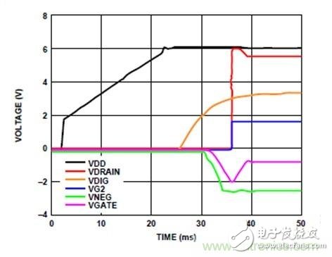
Figure 13. HMC981LP3E Power Rail Enable Sequence
Adjust the default VNEG and VGATE thresholds
The typical value of VNEG is −2.46 V, as shown in Figure 14. Due to the internal logic of the HMC980LP4E, this default value limits the VGATE output voltage swing capability of the HMC980LP4E.
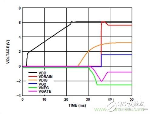
Figure 14. VNEG defaults
With the default configuration, the VGATE typical output swing is between −2 V and 0 V. but,
◠Some DUTs may require a gate voltage less than −2 V.
◠Some DUTs have an absolute maximum gate voltage rating (AMR) greater than −2.1 V, for example −1.5 V. In this case, the typical gate voltage of the DUT is required to be higher than the AMR value of VGATE, for example −1 V. However, during power-up, the VGATE output of the HMC980LP4E always drops to a typical value of −2 V.
By adjusting the default values ​​of VNEG and VGATE with an external resistor, both of these problems can be solved simultaneously. The resistors R5, R6, R7 and R8 shown in Fig. 15 are used for this purpose.
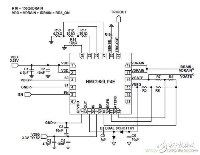
Figure 15. External resistors used to adjust the default values ​​of VNEG and VGATE
If VNEG < −2.46 V is required, then R5 (kΩ) = open and R6 (kΩ) = 50/(50 × (required VNEG − 0.815) / (262 × (0.815 − 1.44)) − 1).
If VNEG > −2.46 V is required, then R5 (kΩ) = 262/(262 × (1.44 − 0.815)/(50 × (0.815 − required VNEG)) − 1), and R6 (kΩ) = open.
If VGATE < −2.46 V is required, then R7 (kΩ) = open and R8 (kΩ) = 50/(50 × (required VGATE − 0.815) / (262 × (0.815 − 1.44)) − 1).
If VGATE > −2.46 V is required, then R7 (kΩ) = 262/(262 × (1.44 − 0.815)/(50 × (0.815 – required VGATE)) − 1), and R8 (kΩ) = open.
During power-up, if VNEG reaches the default value of −2.46 V, VNEG is enabled. Therefore, the VNEG value must be less than the VGATE value.
It is recommended to configure the VNEG value of the HMC980LP4E to be greater than −3.5 V.
For example, if VNEG = −1.5 V and VGATE = −1.3 V, then R5 = 631 kΩ, R7 = 477 kΩ, R6 = R8 = open. In addition, if VNEG = -3.2 V and VGATE = -3 V are required, then R6 = 221 kΩ, R8 = 303 kΩ, and R5 = R7 = open.
Reduce VGATE rise time
There is a delay between when the enable signal reaches the active bias controller enable pin and when the VGATE voltage level of the DUT VGATE input pin establishes the desired value. This delay is caused by the internal propagation delay of the bias controller and the settling time of the VGATE signal. The shunt capacitor used on the connection between the active bias controller VGATE output and the DUT VGATE input pin can affect the VGATE settling time. The HMC980LP4E typical enable waveform (see Figure 16) indicates that the VGATE settling time is greater than 1 ms.
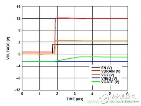
Figure 16. HMC980LP4E Typical Enable Waveform
External circuitry can affect the gate rise time without affecting the propagation delay. Figure 17 shows a typical VGATE connection between the HMC980LP4E and the DUT amplifier. The shunt capacitor C1 is typically used on the VGG pin of the amplifier. R1 is typically 0 Ω, which is not used.
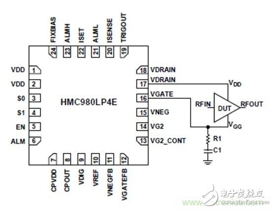
Figure 17. VGATE Connection Circuit Between HMC980LP4E and DUT
When C1 = 10 μF, the typical rise time is greater than 1.5 ms (see Figure 18). When C1 is reduced to 1 μF, the rise time is reduced to 131 μs (see Figure 19).
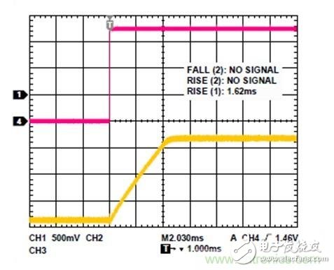
Figure 18. Typical VGATE rise time at C1 = 10 μF
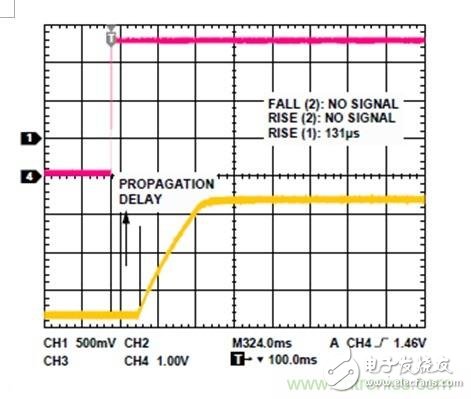
Figure 19. Typical VGATE rise time at C1 = 1 μF
When C1 = 100 nF, the VGATE rise time is reduced to 15.5 μs, but overshoot can cause ringing (see Figure 20). Adding a series resistor R1 with a value of 68 Ω to C1 = 100 nF improves the response performance and keeps the rise time at a similar level (see Figure 21).
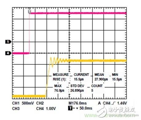
Figure 20. Typical VGATE rise time at C1 = 100 nF
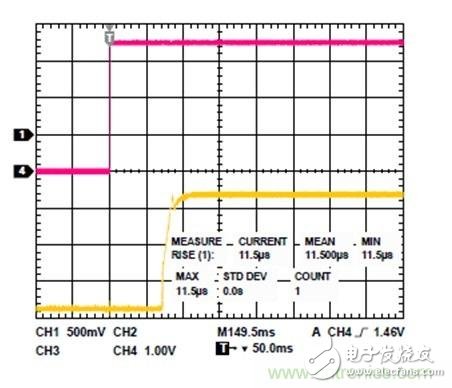
Figure 21. Typical VGATE rise time for C1 = 100 nF and R1 = 68 Ω
Daisy chain configuration
When multiple active bias controllers bias multiple DUTs, they can be configured in a daisy-chain configuration. The active bias controller generates the TRIGOUT output when the VDRAIN, VG2, and VGATE outputs are asserted. Using the TRIGOUT signal to enable another bias controller via the enable pin (EN) can increase system safety. There are many applications for daisy chain configuration, and Figure 22 and Figure 23 show two applications. The number of DUT stages and bias controllers can be increased.
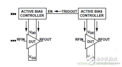
Figure 22. Daisy-chain configuration of two amplifiers in cascade configuration
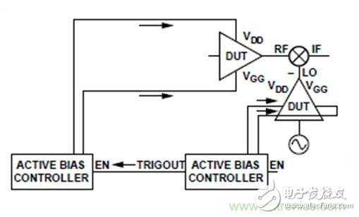
Figure 23. Daisy-chain configuration of DUT amplifiers on different signal paths
Figure 24 shows the VDRAINx and VGATEx responses of two active bias controllers in a daisy-chain configuration, with each bias controller powering one DUT. The second bias controller is enabled by a trigger signal provided by the first bias controller. This architecture ensures that the second DUT is enabled after the first DUT is enabled.
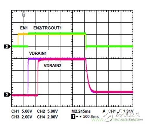
Figure 24. VDRAINx response of two active bias controllers in a daisy-chain configuration, each bias controller powering a DUT
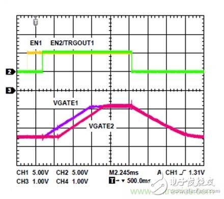
Figure 25. VGATEx response of two active bias controllers in a daisy-chain configuration, each bias controller powering a DUT
Test the function of the active bias controller
The VDRAIN and VGATE outputs of the active bias controller can bias the DUT, such as a FET or amplifier with external bias requirements. Once the DUT is connected to the bias controller, the feedback loop is closed and the bias controller is operational.
For active bias controllers with a fixed load (such as a resistor), the function cannot be tested because the loop is not closed.
Although testing an active bias controller without a DUT does not provide useful information, the following diagnostic checks can be performed.
◠When IDD = 0 mA, the voltage drop across the VDD input and VDRAIN output is negligible; therefore, VDRAIN is almost equal to VDD. ◠VNEG is typically −2.46 V. ◠The maximum VGATE is VNEG + 4.5 V, and the typical value is 2.04 V.
For other bias controllers, these values ​​are available in the data sheet.
Bias multiple DUTs with a single active bias controller
A single active bias controller can be utilized to bias two or more DUTs. For this reason, the total drain current of the DUT should be considered when calculating the RSENSE value.
However, it should be noted that using this method limits the advantages of the active bias controller for the following reasons:
â— Active bias controllers cannot compensate for gate voltage differences between devices common to GaAs devices. Therefore, the two devices may be biased with the same gate voltage to achieve optimum performance.
â— If a DUT consumes excessive current due to a short circuit or other fault, the bias controller turns off all biased DUTs. Although this will not damage the device, it will affect system functionality.
Active bias controller circuit example
Offset HMC460LC5 with HMC981LP3E
To offset the HMC460LC5 with the HMC981LP3E, perform the following procedure:
◠Set R10 to 426 Ω to set the IDD of the HMC981LP3E to 75 mA. A common resistance value of 430 Ω can be used.
â— Calculate the VDD value to 8.75 V.
• Use R4 and R6 to ensure that the VGATE voltage is within the absolute maximum ratings given in the HMC981LP3E data sheet. See the “Adjusting the Default VNEG and VGATE Thresholds†section for details.
â— The VGG shunt capacitor value can be reduced to increase the rise time (see HMC460LC5 in Figure 26). See the section "Reducing VGATE rise time" for details.
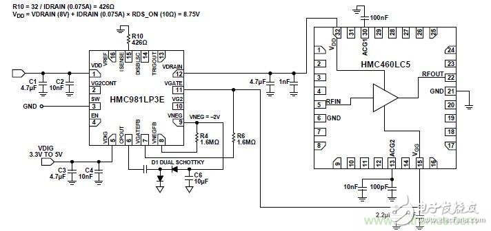
Figure 26. Application circuit for biasing HMC460LC5 with HMC981LP3E
Offset HMC1082LP4E with HMC980LP4E
To offset the HMC1082LP4E with the HMC980LP4E, perform the following procedure:
◠Set R10 to 680 Ω to set the IDD of the HMC980LP4E to 220 mA.
â— Calculate the VDD value to 5.62 V.
• Use R5 and R7 to ensure that the VGATE voltage is within the absolute maximum ratings given in the HMC980LP4E data sheet. See the “Adjusting the Default VNEG and VGATE Thresholds†section for details.
â— The VGG shunt capacitor value can be reduced to increase the rise time (see HMC1082LP4E in Figure 27). See the section "Reducing VGATE rise time" for details.
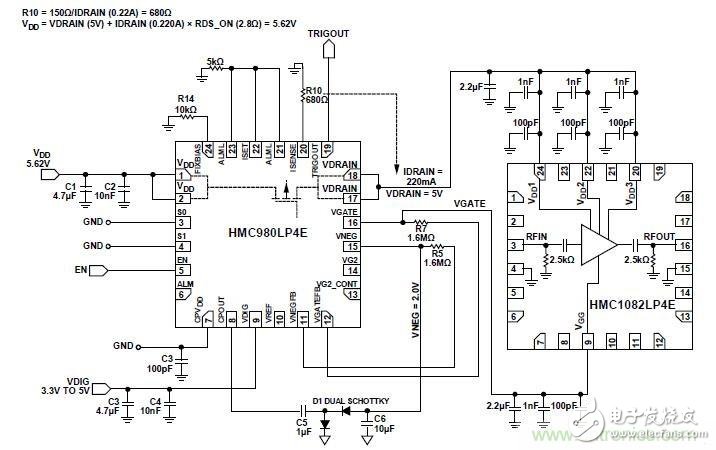
Figure 27. Application Circuit for Biasing the HMC1082LP4E Using the HMC980LP4E
* Offset HMC659LC5 with HMC980LP4E *
To offset the HMC659LC5 with the HMC980LP4E, perform the following procedure:
◠Set R10 to 500 Ω to set the IDD of the HMC980LP4E to 300 mA.
◠Use a common resistance value of 510 Ω.
â— Calculate the VDD value to 8.84 V.
â— Set VGG2 of HMC980LP4E with R3 and R4.
• Use R5 and R7 to ensure that the VGATE voltage is within the absolute maximum ratings given in the HMC980LP4E data sheet. See the “Adjusting the Default VNEG and VGATE Thresholds†section for details.
â— The VGGx shunt capacitor value can be reduced to increase the rise time (see HMC659LC5 in Figure 28). See the section "Reducing VGATE rise time" for details.
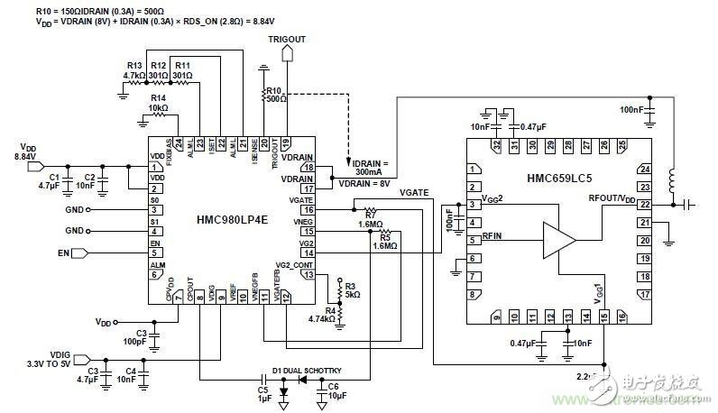
Figure 28. Application Circuit for Biasing the HMC659LC5 Using the HMC980LP4E
* Offset HMC659LC5 with HMC920LP5E *
To offset the HMC659LC5 with the HMC920LP5E, perform the following procedure:
◠Set RSENSE to 549 Ω to set the IDD of the HMC920LP5E to 300 mA.
◠Set R8 to 30.9 kΩ to set VDRAIN = 8 V.
◠Use R20 and R22 to ensure that the VGATE voltage is within the absolute maximum ratings given in the HMC920LP5E data sheet. See the “Adjusting the Default VNEG and VGATE Thresholds†section for details.
â— The VGGx shunt capacitor value can be reduced to increase the rise time (see HMC659LC5 in Figure 29). See the section "Reducing VGATE rise time" for details.
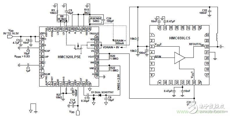
Figure 29. Application Circuit for Biasing the HMC659LC5 with the HMC920LP5E
in conclusion
During power-up and power-down, follow the recommended bias sequence of the external biasing device to ensure device safety. Operating the amplifier with an active bias controller ensures that the device operates at the correct timing and at the desired level, improving overall system performance.
ADI's family of active bias controllers can handle the biasing requirements of externally biased RF/microwave devices such as FETs, amplifiers, frequency multipliers, optical modulator drivers, and frequency converters. The gate voltage of the DUT is adjusted by closed loop feedback to provide the desired drain current. The timing control features of the bias controller's VGATE, VDRAIN, and VGG2 outputs ensure that the DUT is well protected during power-up and power-down.
Chongqing LDJM Engine Parts Center , https://www.ckcummins.com