1 Introduction
GaN is a semiconductor material with a wide band gap and a direct band gap of 3.39 eV, which is resistant to high temperatures and corrosion. Due to its realized, potentially even revolutionary commercial value, there has been a wave of GaN research around the world [1, 2]. Some test instrument manufacturers have also quickly introduced new devices, such as ACCENT, which introduced the PN4400ECV device for wide bandgap materials. It can be used not only to measure the longitudinal carrier concentration distribution of GaN epitaxial layers, but also provides many other functions, such as IV, CV, DP (depletionprofile), etc., which can provide a lot of information for material growth and analysis. It would make sense to fully utilize this information and finally match the LED chip results one by one. However, when used on GaN, the instrument is a brand new one, lacking experience, and it takes a lot of verification to do one-to-one correspondence. At present, this paper only attempts to discuss the longitudinal distribution of carrier concentration in relation to crystal growth and quality. It is well known that the electron injecting layer in a GaN-based LED epitaxial structure is typically a silicon doped n-type layer. With the development of GaN growth technology, the silicon-doping technology is also improving. Some manufacturers deliberately interrupt the doping of silicon or reduce the doping of silicon to form a current spreading layer during the silicon doping process; some also dope silicon in the barrier layer. Therefore, the diffusion behavior of silicon in GaN has been concerned. In addition, the p-type layer on the quantum well in the LED structure has a high growth temperature. What is the diffusion width of silicon during the p-layer growth process? Will silicon diffuse through the quantum well to the p-layer to the silicon in the barrier layer? Will it spread? These issues are worthy of serious discussion. However, due to the recent rise of such semiconductor materials, there have been few reports on the diffusion of silicon in GaN. In [3], SIMS was used to study the diffusion of substrate silicon into GaN in unintentionally doped GaN grown on SOI. The diffusion mechanism was speculated and the effect of silicon diffusion on material properties was discussed. The diffusion width w of silicon in the substrate to the GaN epitaxial layer was measured to be about 0.5 Lm (the sample was grown at 940e for 1 h). Reference [4] relates to the diffusion behavior of oxygen at the interface of GaN/Al2O3. ECV measurement is used. In combination with other measurement methods, oxygen is considered to diffuse several hundred nm. In contrast to GaN, there has been a lot of literature research on the diffusion behavior of silicon in GaAs, and it has done a lot of work in mechanism research, theoretical calculations, and the use of various detection methods [5 ], this has important reference value for GaN. In this paper, the diffusion of silicon is studied by measuring the concentration distribution of longitudinal carriers in the GaN epitaxial layer.
2 experiment
The experimental samples were silicon-doped GaN epitaxial wafers grown in a production MOCVD system with a densely coupled nozzle reactor manufactured by THOMASSWAN, UK. Table 1 shows the growth parameters of the two samples A and B.
Table 1 Growth parameters of MOCVD grown GaNBSi samples A and B on Al2O3 (0001) substrates
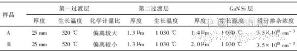
The main difference between the two samples A and B is that the buffer layer growth process is different. Figure 1 is a growth process diagram before 6000s, representing the buffer layer growth process used when the corresponding sample is grown on an imported MOCVD device. Figure 1 is not a real-time reflectance curve for the sample. Sample A uses deviated stoichiometric GaN as a low temperature and high temperature buffer layer with thicknesses of 25 nm and 400 nm, respectively. After growth of the high temperature buffer layer, GaN epitaxial growth is performed. In the growth curve of sample A of Fig. 1, the long-term low-reflectivity section corresponds to the high-Ga high-temperature buffer layer growth process. Sample B did not use a stoichiometric ratio of GaN as a low temperature and high temperature buffer layer, but directly proceeded to GaN growth after recrystallization of the low temperature buffer layer.
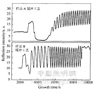
Figure 1 Buffer layer process used for MOCVD growth of GaN samples A and B
The ECV measurement was performed using an ACCENT PN4400ECV analyzer, which is a tester for analyzing the longitudinal carrier concentration distribution of wide bandgap materials based on the addition of the PN4300PC. The capacitance C is measured using a carrier frequency of 3 kHz, and the differential dC/dV of the capacitance versus voltage is measured using a 40 Hz frequency modulation.
GaN is a corrosion-resistant material, and it is not easy to achieve uniform peeling of one layer. We chose 1mol/L H2SO4 as the etching solution. It has been found that even a self-made epitaxial layer with a complete LED structure can occasionally be uniformly etched; for a silicon-doped n-type GaN epitaxial layer, reproducible, uniform, and clear outline can be obtained by uniform irradiation and limitation of ultraviolet light. Corrosive surface. But this must also be carefully chosen to corrode voltage and light intensity, so that the etching current is appropriate, and pay attention to avoid the avalanche area. It is particularly noteworthy that although the PN4400 is equipped with a device that automatically eliminates bubbles generated on the corroded surface, it is still difficult to automatically and effectively remove the bubbles, which seriously affects the uniformity of the corrosion and the correctness of the measurement results. To this end, corrosion must be suspended frequently, manual intervention, and injection of needles to spray H2SO4 to remove air bubbles. As long as you pay attention to these, it is not difficult to obtain a uniform corrosion pit. Fig. 2 is a differential interference micrograph of the sample A after being etched, having a corrosion depth of 2 μm, a circular area of ​​about 0.098 cm 2 , and uniform etching.
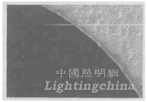
Fig. 2 Differential interference micrograph of corrosion pit of sample A (corrosion depth 2Lm, round area 0.098cm2, @100)
The corresponding blue chip of the two buffer layer processes is provided by Jiangxi Xinlei Company.
3 Results and discussion
3.1 Measurement results
Fig. 3 and Fig. 4 are longitudinal distributions of carrier concentrations of two samples A and B measured by an ECV analyzer. A depth of zero indicates the surface of the epitaxial layer. The longitudinal distribution of the carrier concentration in the two figures is consistent and can be divided into four segments, which are represented by (a), (b), (c) and (d), respectively. This article analyzes the four segments as follows.
(a) The curve is basically straight, and the measured carrier concentration is between (3~4) @×1018cm-3, which is consistent with the designed carrier concentration of 3.5×1018cm-3. Corresponding to the laser interferometry of the thickness of the silicon-doped layer in the layer structure, it indicates that this segment is a silicon-doped layer of GaN.
(b) The slope corresponds to the diffusion of silicon (the cause of which is discussed).
(c) Corresponding to the undoped GaN layer, as the thickness of the undoped GaN layer increases, the background carrier concentration decreases gradually, and the corresponding crystal quality is improved with the increase of the growth thickness [6]. However, this improvement will be saturated. Therefore, in order to save costs, when the background carrier concentration is low, the growth of the layer can be stopped in time, and the silicon doping is transferred. The valley between b and c can be used to indicate the quality of the crystal. The background carrier concentration of Sample A was smaller than that of the sample, indicating that the crystal quality was good. As we all know, the reverse current of LED can directly reflect the quality of crystal growth. For the same LED chip process, the buffer layer process of sample A was used, and the current at 10V reverse voltage was 10LA. With the buffer layer process of sample B, the current at the reverse voltage of 6V is already 25LA. It can be seen that the ECV test can not only provide reference for the optimization of growth process parameters, but also can be used to evaluate the quality of the epitaxial wafer before the chip is fabricated.
(d) Corresponding to the vicinity of the substrate.
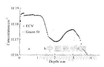
Figure 3: Longitudinal distribution of carrier concentration and Gaussian fit of sample A (a) silicon doped segment; (b) diffused segment; (c) undoped silicon segment; (d) near substrate
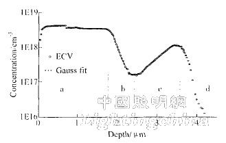
Figure 4: Longitudinal distribution of carrier concentration and Gaussian fit of sample B (a) doped silicon segment; (b) diffusion segment; (c) undoped silicon segment; (d) near substrate
3.2 Gaussian fitting and diffusion coefficient of silicon
After doping silicon, silicon is diffused toward the sapphire substrate (ie, segment (b)). The main diffusion model is used for the test in paragraph (b), assuming that the distribution of impurities satisfies the Gaussian distribution [5], that is, satisfy:
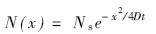 (1)
(1)
Ns is originally the impurity concentration of the semiconductor surface, which can be considered as the carrier concentration of (a) segment; t is the diffusion time, and the growth time of the two samples is different, that is, the diffusion time is somewhat different. The growth time of sample A is shorter, which is reflected in the figure, that is, the slope of Fig. 3(b) is larger than that of Fig. 4, that is, the silicon diffusion area is narrower; D is the diffusion coefficient; in the case of uniform corrosion (for the sample) A has done five kinds of corrosion depth metallographic microscopy observations, the results show that the corrosion is very uniform), this paper on the corresponding diffusion section of Figure 3, 4 Gaussian simulation, the expression is:
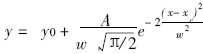 (2)
(2)
Where: w is the peak width parameter, ie the diffusion width.
The simulation results are shown in Figure 3, the smooth line of the 4(b) zone (the one that was interrupted at the bottom of the valley). The degree of coincidence between the simulation results and the measurement results is quite good, indicating that a diffusion model with Gaussian distribution can be used, and equation (2) can be used as an empirical formula. According to the normalization principle, the formula (2) shows the starting point of silicon doping. 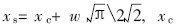 The peak position coordinates in equation (2) are shown in the simulation parameters listed in Figures 3 and 4; the calculation results of xs are shown in Table 2, which corresponds to the silicon-doped layer measured by the laser interferometer in Table 1. Thickness, the degree of conformity between the two is good, and it also indicates that the model selection is reasonable. From the parameter w obtained by the simulation, the diffusion coefficient D at the corresponding temperature can be obtained according to the formulas (1), (2) and the corresponding growth time, as shown in Table 2. The growth time after the start of silicon doping in the table is found by the real-time curve of the reflectance of the laser interference epitaxial layer during the growth of the material.
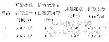
It can be seen from Table 2 that the diffusion coefficients D of the two samples A and B are the same, and the diffusion widths w are 0.32 Lm and 0.35 Lm, respectively. In [3], the diffusion of silicon into GaN in a non-doped GaN grown on SOI (Siliconon Insulator) was measured using SIMS. The sample was obtained by growing at 940e for 1 h, and the measured diffusion was obtained. The width w is about 0.5 Lm. Considering that they measured the situation near the substrate, the crystal quality here is not good, and the diffusion of impurities is naturally more intense. Therefore, the results are comparable to the results of this paper (Table 2).
Table 2 Silicon diffusion coefficient D and silicon-doped starting point Xs in samples A and B