1. Application significance of ASI interface
This article refers to the address: http://
With the rapid development of digital TV technology, digital processing has been realized in a large part of the production and design of TV programs. In terms of the transmission of the program, we have been able to receive multiple sets of digitally compressed coded programs from the satellite. This transmission method not only ensures the high-definition quality of the program, but also greatly reduces the cost of transmission, transmission and reception of the television program. A large number of transceivers use ASI's interface standard, which is designed to implement transceivers for TV program transmission streams based on PC and ASI interface standards. It has a large number of applications in the production, storage and replay of programs.
With the development of digital broadcasting, the digitization of cable TV is getting faster and faster. The digital technology has improved the technical quality and program quality of radio and television programs, provided multimedia service means for broadcasting and television and integrated data services, and broadened the broadcasting and television services. After digitization, the TV signal transmission adopts the MPEG-2 video coding standard, and can transmit high-definition television programs with a bandwidth of 4 to 5 Mbit/s. The noise is not accumulated, and the transmission quality is greatly improved, and has a broad application prospect. In current digital communication systems, there are two MPEG-2 interface standards: the ASI asynchronous serial interface and the SPI synchronous parallel interface. The SPI interface has a total of 11 useful signals, each of which is differentially divided into two channels to improve the transmission immunity, and is transmitted by DB25 on the physical link. Due to its simple processing and high scalability, the input and output of the MPEG-2 codec and video test equipment generally use the SPI interface. However, due to its many connections and complexity, the SPI interface can only be used for short-distance transmission. ASI (Asynchronous Serial Interface) requires only one cable to achieve 270 Mbit/s transparent transmission, so the application is very common. The ASI interface has the advantages of high speed, reliability, fixed baud rate and long transmission distance, and the connection is simple and low cost, and can be widely applied to various high-speed point-to-point transmissions, especially video transmission equipment.
2. ASI protocol structure
ASI can have different data reception rates, but the transmission rate is constant at 270 Mbit/s. Therefore ASI can send and receive MPEG-2 data at different rates. ASI adopts a hierarchical structure and is divided into three layers: a physical layer, a data encoding layer, and a transport rule layer.
The zeroth layer is the physical layer. The physical layer defines the transmission medium, the driver and receiver, and the transmission rate. The physical interface provides LED-driven multimode fiber and coaxial cable. The base rate is defined as 270 Mbps. In coaxial cable applications, the maximum allowable jitter is specified in a conventional manner of random and data-dependent jitter and duty cycle distortion.
The first layer is the data encoding layer. DC balanced 8B/10B transmission code. This code converts each 8-bit data byte into a l0bit codeword with the following characteristics: the run length is equal to or less than 4 bits; This code provides error checking by invalid transmission code points and "run" inequalities. Dedicated characters are specified as additional code points beyond the need to encode data bytes. In particular, the comma character (defined as K28.5-specific characters in the 8B/10B transport code rule) is used to establish byte alignment in the DVB-ASI transport link. The byte is 8B/10B encoded at the transmitting end, and a 10-bit codeword is generated for each 8-bit byte that appears, so that these 10-bit codewords are converted by parallel/serial conversion at a fixed output bit rate of 270 Mbps. If the parallel/serial converter requests a new codeword, but the data source is not yet ready for a new codeword, the sync word (or comma character K28.5) should be inserted. Inserting a sync character in the spare field of the transmitted data enables the transmission code to have strong anti-interference, error detection and synchronization capability.
The second layer is the transport rule layer. The Layer 2 standard for ASI transmission uses the MPEG-2 Transport Stream Packet (TS) as the basic unit of information. Transport packets can be transmitted in three ways: one is a block-wise continuous byte transfer, that is, the sync byte is not inserted in the transport stream of a single packet; the second way is a separate byte. Mode transfer, in which synchronous bytes are inserted; the third way is a combination of consecutive bytes and sync bytes. In addition, ASI's Layer 2 protocol stipulates that there must be at least two sync words (K28.5) before each transport packet. Although the packet synchronization process is not defined by the ASI transport protocol, the MPEG-2 transport packet sync byte (47H) is included in the layer 2 packet definition so that the receiving device can implement packet synchronization. The Layer 2 definition of the ASI interface uses the syntax of the MPEG-2 transport stream, but adds the additional requirement of requiring at least two K28.5 sync characters before each transport packet. As long as it is initially synchronized, the 8B/10B receiving device is generally capable of maintaining synchronization without the need to add sync characters. However, when external factors such as line interference cause loss of synchronization, the increased sync byte can resynchronize a transport packet. The transport packet structure shall comply with the provisions of EN/ISO/IEC 13818-1 and ETS 300 429 for transport stream packets. The packet length can be 188 bytes or 204 bytes. Transport packets can appear on Layer 2 in two ways. The first type of 188 bytes in each TS packet is contiguous and is divided into three parts: the packet header, the adjustment field, and the payload. The adjustment field is optional, and not all adjustment fields appear in the transport stream group. The sync character is inserted between the two packets, called burst mode. The transmission of TS stream is realized by burst mode, which has the flexibility of dynamic allocation, scalability, scalability, strong anti-interference, etc. The second is that the synchronization word is randomly and evenly inserted between TS data. , called non-burst mode.
3. Design implementation
3.1 ASI Send Card Hardware Design
Most ASI encoding implementations use Cypress's CY7B923 to convert parallel data to serial data. CY7B923 mainly implements 8/10bit conversion of codewords, inserts synchronization word K28.5 and parallel/serial conversion. The transmission rate of ASI is constant at 270MHz, and the input MPEG-2 TS rate is different. Therefore, to achieve rate matching with FIFO, it is necessary to logically control the communication between the input SPI data, FIFO and CY7B923. Considering the comprehensive performance, price and program complexity, this solution uses FPGA and uses Verilog programming to realize the logic control between them. Altera's ASI IP core is used instead of Cypress's CY7B923 to realize ASI data encoding. The ASI IP core has the advantages of ease of use and low cost.
In the ASI encoding process, only the 8-bit data of the MPEG-2 encoded TS stream and the one-bit TS rate transmission clock are input to the FPGA. This scheme is the PCI 33M clock signal. Because in this scheme, the TS format transmits data in burst mode of 188 bytes, according to the data valid signal DVALID, the FPGA detects this signal to determine when it is valid data to receive TS stream data without concern for TS. The sync header of the code stream. The FPGA writes the received data to the FIFO with the TS rate clock. When the FIFO is half full, the FPGA receives a half full signal from the FIFO, then the FPGA issues a FIFO readable signal to the ASI core, and the ASI core reads the data in the FIFO at 27 Mbps; when the FPGA counts up to the ASI core, a certain number of FIFOs are read. Data, the FPGA sends a FIFO unreadable signal to the ASI IP core to prevent FIFO read. The MPEG-2 transport rate has a parallel maximum speed of 132 Mbps and a read FIFO rate of 27 Mbps, so the FIFO will overflow. Therefore, when sending an MPEG-2 transport stream, there is a driver that controls how much data is sent at a time. Considering the delay, this scheme burns a 2K asynchronous FIFO inside the FPGA. When the ASI IP core is unreadable in the FIFO, the ASI code stream is filled with K28.5 to maintain a fixed transmission rate of 270 Mbps. Finally, the serial data is transmitted and transmitted over the coaxial cable. In this scheme, the insertion of the sync word K28.5 adopts the manner in which the single byte of the transport stream cannot be K28.5 sync words before and after.
The hardware implementation block diagram of the ASI sending card is as follows: 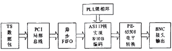
The system is based on ALTERA's FPGA chip, the Cyclone II EP2C8Q208. The encoded parallel data stream is fed into the asynchronous FIFO via the PCI bus. Asynchronous FIFO mainly implements data buffering and clock matching. The system performs a DMA operation to send data to the board. The FIFO caches this data to avoid data loss. Also, the clock has a PCI 33M clock signal and a 27M ASI input clock signal. This requires synchronizing the clocks of these two different frequencies. The FIFO operates at two different clocks, with different clocks for the input and output of the data. This achieves clock isolation and seamless connectivity. The FIFO uses a 32-bit input and an 8-bit output, which are consistent with the data width of the PCI and the input data width of the ASI IP core. The ASI IP core implements 8-bit data to 10-bit encoding. The reference clock of the ASI IP core is 27M, and the output clock is 270M. With an external phase-locked loop, the 27MHz clock frequency is generated by a crystal oscillator, and a 270M clock is generated through the phase-locked loop for data output of the ASI interface. The PE65508 is coupled and impedance matched and finally sent out via the BNC plug.
3.2 Generation of ASI IP cores
The implementation of ASI encoding is directly generated by Quartus 6.1 for simulation verification.
Generation of the ASI interface. The IP core first needs to be installed and can be downloaded from the Altera website. After installation, open the Quartus 6.1 new project, click Megachazard plug-in Maneger in the tools menu, choose to create a new macro function variable, and step by step to generate the asi file. The device and file generation languages ​​can be selected, with the Cyclone II and verilog languages ​​selected. It should be noted that the generated file name must match the top file name of the project. Select Transmitter, here as the sending interface. In ASI, depending on the speed of the selected device, you can choose whether to generate a phase-locked loop. An external phase-locked loop is used here to generate an output frequency of 270MHz.
The generated ASI interface verilog part of the code is as follows:
Module asi ( rst, tx_refclk, tx_data, tx_en, tx_clk270, asi_tx);
Input rst,tx_refclk,tx_en,tx_clk270,asi_tx;
Input [7:0] tx_data;
Asi_megacore_top asi_megacore_top_inst( .rst(rst), .tx_refclk(tx_refclk), .tx_data(tx_data),
.tx_en(tx_en), .tx_clk270(tx_clk270), .asi_tx(asi_tx));
......
Endmodule
This interface implements encoding of 8-bit data to 10-bit data. The 8-bit MPEG-2 data is input from the input and flows into the internal FIFO. Tx_data 8-bit parallel data input interface for data encoding, which converts each 8-bit data into 10-bit data; then the serializer converts 10-bit parallel data into serial data. Asi_tx The encoded serial data input interface. If the transmission rate of the MPEG-2 TS stream is less than 270 Mbps, it is necessary to insert a sync character to ensure a stable 270 Mbps output. Tx_refclk is the input 27M reference clock and tx_clk270 is the 270M data output clock. They are obtained through an external phase-locked loop. Rst is the reset signal and the high level is the active level, causing the entire design to stop working. The tx_en data input enable signal controls the data to be encoded in the FIFO to enter the ASI IP core for data encoding and parallel-to-serial conversion.
3.3 ASI Engineering and Simulation Waveforms
In the own project of adding the generated ASI kernel, the top-level part of the code is as follows:
Module FIFO_ASI(clk27,data,t_out);
Input clk27;
Output data,t_out
Wire clk13,clk270;
Wire[31:0] data32;
Wire[7:0] data8;
......
Endmodule
Simulate it, the waveform is as follows: 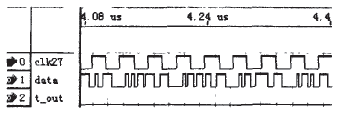
The external 27M clock is connected to clk27 as the input reference clock for the ASI IP core 27M. T_out is a clock output signal, which is divided by 27M and used as an indicator signal to monitor whether the program is downloaded to FPAG. When the indicator light is normally flashing, it indicates that the program has been lowered into the chip and can work. ASI data encoded by the ASI IP core is input by data. In this project, the TS stream is continuously sent to the board through a computer, and after ASI encoding, it is output through the ASI interface. At the receiving end, through an ASI receiving card, the received data is read out, and it can be seen that the ASI is working normally. In the burst mode when the TS stream is sent, the data read is as follows: 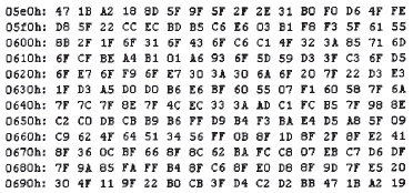
During the debugging phase, the PC continuously transmits the same MPEG-2 encoded TS packet. In the received data, a continuous MPEG-2 encoded TS packet can be seen and is identical to the transmitted data. The reception of the TS packet uses an ASI receiving card as the receiving end, and is input to the computer through the USB interface, and is displayed after reading the data with the corresponding software.
4. Application significance
The DVB-ASI card based on Altera's ASI IP core designed in this paper implements the correct encoding and transmission of ASI data. Implementing logic control and data caching with FPGA can easily implement system upgrade and realize the transmission of multiple ASI data. Compared with the ASI transmission card implemented by Cypress's CY7B923, this card is more suitable for mass production, which can save costs, improve market competitiveness, and has a good market prospect.
The author's innovative view is to replace Cypress's CY7B923 dedicated ASI transmit chip with Altera's ASI IP core to achieve stable transmission of ASI data. This solution reduces cost, is flexible in design, and is easy to upgrade to multiple ASI data transmissions.
In-ear earphones are sometimes referred to as earbuds, and they refer to earphoees that are small enough to fit into the ear. The Sport Earphone are written with L and R, L is left for the left channel, and R is the right for the right channel. In principle, the thinner the earmuffs, the more comfortable they are. However, the thin earmuffs will be less soundproof.
Correct use:
1: Set the volume of the source to the minimum.
2: Insert the 3.5mm plug of the in-ear earphone into the earphone jack.
3: Adjust the volume to a position that sounds comfortable. In-ear earphones are not recommended for driving motorcycles, bicycles, operating machines, and jogging, as you may affect your judgment of potential hazards.
4: Do not open the volume too much during use.
5: When pulling the earphone plug, you should pinch the hard plastic part of the back end of the plug and pull it out, instead of pulling it straight out through the wire.
6: Avoid excessive bending of the wire for a long time.

In Ear Headphones,Sport Earphone,In Ear Earphones,Zipper In Ear Headphones
Shenzhen Linx Technology Co., Ltd. , http://www.linxheadphone.com